TPA3116D2
TPA3118D2
TPA3130D2
SLOS708B –APRIL 2012–REVISED MAY 2012
www.ti.com
These devices have limited built-in ESD protection. The leads should be shorted together or the device placed in conductive foam
during storage or handling to prevent electrostatic damage to the MOS gates.
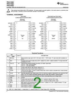
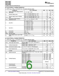
TERMINAL ASSIGNMENT
TPA3116D2
TPA3130D2 and TPA3118D2
32-PIN HTSSOP PACKAGE (DAD)
32-PIN HTSSOP PACKAGE (DAP)
PACKAGE
(TOP VIEW)
PACKAGE
(TOP VIEW)
1
2
32
31
30
29
28
27
26
25
24
23
22
21
20
19
18
17
PVCC
PVCC
BSPR
OUTPR
GND
1
32
31
30
29
28
27
26
25
24
23
22
21
20
19
18
17
PVCC
PVCC
BSPR
OUTPR
GND
MODSEL
SDZ
MODSEL
SDZ
2
3
FAULTZ
RINP
3
FAULTZ
RINP
4
4
RINN
5
RINN
5
PLIMIT
GVDD
GAIN/SLV
GND
6
OUTNR
BSNR
GND
PLIMIT
GVDD
GAIN/SLV
GND
6
OUTNR
BSNR
GND
7
7
8
8
Thermal
PAD
Thermal
PAD
9
BSPL
OUTPL
GND
9
BSPL
OUTPL
GND
LINP
10
11
12
13
14
15
16
LINP
10
11
12
13
14
15
16
Top
Bottom
LINN
LINN
MUTE
AM2
OUTNL
BSNL
PVCC
PVCC
AVCC
MUTE
AM2
OUTNL
BSNL
PVCC
PVCC
AVCC
AM1
AM1
AM0
AM0
SYNC
SYNC
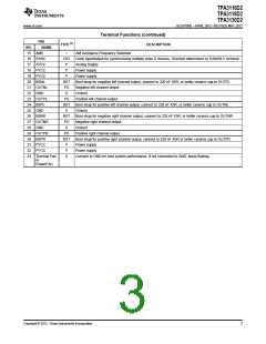
Terminal Functions
PIN
TYPE(1)
DESCRIPTION
NO.
NAME
1
2
3
MODSEL
I
Mode selection logic input (LOW = BD mode, HIGH = 1 SPW mode). TTL logic levels with compliance to
AVCC.
SDZ
I
Shutdown logic input for audio amp (LOW = outputs Hi-Z, HIGH = outputs enabled). TTL logic levels with
compliance to AVCC.
FAULTZ
DO
General fault reporting including Over-temp, DC Detect. Open drain.
FAULTZ = High, normal operation
FAULTZ = Low, fault condition
4
5
6
RINP
I
I
I
Positive audio input for right channel. Biased at 3 V.
Negative audio input for right channel. Biased at 3 V.
RINN
PLIMIT
Power limit level adjust. Connect a resistor divider from GVDD to GND to set power limit. Connect directly
to GVDD for no power limit.
7
GVDD
PO
Internally generated gate voltage supply. Not to be used as a supply or connected to any component other
than a 1 µF X7R ceramic decoupling capacitor and the PLIMIT and GAIN/SLV resistor dividers.
8
9
GAIN/SLV
GND
I
G
I
Selects Gain and selects between Master and Slave mode depending on pin voltage divider.
Ground
10 LINP
11 LINN
12 MUTE
Positive audio input for left channel. Biased at 3 V. Connect to GND for PBTL mode.
Negative audio input for left channel. Biased at 3 V. Connect to GND for PBTL mode.
I
I
Mute signal for fast disable/enable of outputs (HIGH = outputs Hi-Z, LOW = outputs enabled). TTL logic
levels with compliance to AVCC.
13 AM2
14 AM1
I
I
AM Avoidance Frequency Selection
AM Avoidance Frequency Selection
(1) TYPE: DO = Digital Output, I = Analog Input, G = General Ground, PO = Power Output, BST = Boot Strap.
2
Copyright © 2012, Texas Instruments Incorporated

 TI [ TEXAS INSTRUMENTS ]