TPA3116D2
TPA3118D2
TPA3130D2
www.ti.com
SLOS708B –APRIL 2012–REVISED MAY 2012
æ
ö2
æ
ç
è
ö
÷
ø
RL
´ V
ç
÷
P
ç
÷
RL + 2 ´ RS
è
ø
POUT
=
for unclipped power
2 ´ RL
(2)
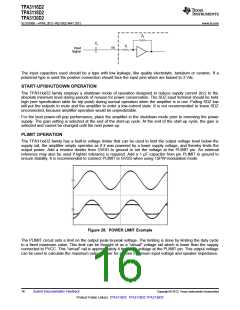
Where:
RS is the total series resistance including RDS(on), and output filter resistance.
RL is the load resistance.
VP is the peak amplitude
VP = 4 × PLIMIT voltage if PLIMIT < 4 × VP
POUT (10%THD) = 1.25 × POUT (unclipped)
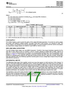
Table 3. POWER LIMIT Example
PVCC (V)
24 V
PLIMIT VOLTAGE (V)(1)
R to GND
Short
R to GVDD
Open
OUTPUT VOLTAGE (Vrms)
GVDD
3.3
17.90
12.67
9.00
24 V
45 kΩ
24 kΩ
Short
51 kΩ
24 V
2.25
GVDD
2.25
1.5
51 kΩ
12 V
Open
10.33
9.00
12 V
24 kΩ
18 kΩ
51 kΩ
12 V
68 kΩ
6.30
(1) PLIMIT measurements taken with EVM gain set to 26dB and input voltage set to 1Vrms
.
GVDD SUPPLY
The GVDD Supply is used to power the gates of the output full bridge transistors. It can also be used to supply
the PLIMIT and GAIN/SLV voltage dividers. Decouple GVDD with a X5R ceramic 1 µF capacitor to GND. The
GVDD supply is not intended to be used for external supply. It is recommended to limit the current consumption
by using resistor voltage dividers for GAIN/SLV and PLIMIT of 100 kΩ or more.
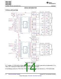
BSPx AND BSNx CAPACITORS
The full H-bridge output stages use only NMOS transistors. Therefore, they require bootstrap capacitors for the
high side of each output to turn on correctly. A 220 nF ceramic capacitor of quality X5R or better, rated for at
least 16 V, must be connected from each output to its corresponding bootstrap input. (See the application circuit
diagram in Figure 27.) The bootstrap capacitors connected between the BSxx pins and corresponding output
function as a floating power supply for the high-side N-channel power MOSFET gate drive circuitry. During each
high-side switching cycle, the bootstrap capacitors hold the gate-to-source voltage high enough to keep the high-
side MOSFETs turned on.
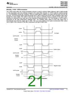
DIFFERENTIAL INPUTS
The differential input stage of the amplifier cancels any noise that appears on both input lines of the channel. To
use the TPA31xxD2 family with a differential source, connect the positive lead of the audio source to the RINP or
LINP input and the negative lead from the audio source to the RINN or LINN input. To use the TPA31xxD2 family
with a single-ended source, ac ground the negative input through a capacitor equal in value to the input capacitor
on positive and apply the audio source to either input. In a single-ended input application, the unused input
should be ac grounded at the audio source instead of at the device input for best noise performance. For good
transient performance, the impedance seen at each of the two differential inputs should be the same.
The impedance seen at the inputs should be limited to an RC time constant of 1 ms or less if possible. This is to
allow the input dc blocking capacitors to become completely charged during the 10 ms power-up time. If the input
capacitors are not allowed to completely charge, there will be some additional sensitivity to component matching
which can result in pop if the input components are not well matched.
Copyright © 2012, Texas Instruments Incorporated
Submit Documentation Feedback
17
Product Folder Link(s): TPA3116D2 TPA3118D2 TPA3130D2

 TI [ TEXAS INSTRUMENTS ]