TMS570LS3137
SPNS162.–SEPTEMBER 2011
www.ti.com
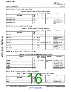
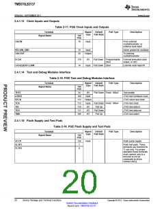
2.4.1.13 Clock Inputs and Outputs
Table 2-17. PGE Clock Inputs and Outputs
Terminal
Signal
Type
Default
Pull State
Pull Type
Description
Signal Name
144
PGE
OSCIN
18
Input
-
-
From external
crystal/resonator, or
external clock input
KELVIN_GND
OSCOUT
19
20
Input
Kelvin ground for oscillator
Output
To external
crystal/resonator
ECLK
119
14
I/O
Pull Down Programmable, External prescaled clock
20uA
output, or GIO.
GIOA[5]/EXTCLKIN
Input Pull Down 20uA
External clock input #1
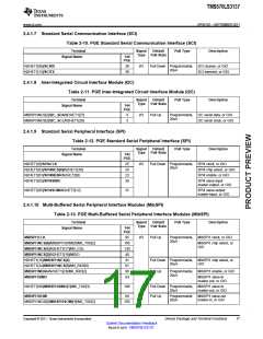
2.4.1.14 Test and Debug Modules Interface
Table 2-18. PGE Test and Debug Modules Interface
Terminal
Signal
Type
Default
Pull State
Pull Type
Description
Signal Name
144
PGE
TEST
nTRST
RTCK
TCK
34
I/O
Input
Output
Input
I/O
Pull Down Fixed, 100uA
Test enable
109
113
112
110
111
108
JTAG test hardware reset
JTAG return test clock
JTAG test clock
-
-
Pull Down Fixed, 100uA
Pull Up
TDI
JTAG test data in
JTAG test data out
JTAG test select
TDO
I/O
Pull Down
TMS
I/O
Pull Up
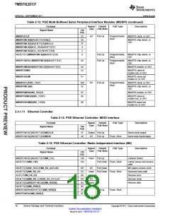
2.4.1.15 Flash Supply and Test Pads
Table 2-19. PGE Flash Supply and Test Pads
Terminal
Signal
Type
Default
Pull State
Pull Type
Description
Signal Name
144
PGE
VCCP
FLTP1
FLTP2
134
7
Input
-
-
Flash pump supply
Flash test pads. These
terminals are reserved for
TI use only. For proper
operation these terminals
must connect only to a
test pad or not be
8
connected at all [no
connect (NC)].
20
Device Package and Terminal Functions
Copyright © 2011, Texas Instruments Incorporated
Submit Documentation Feedback
focus.ti.com: TMS570LS3137

 TI [ TEXAS INSTRUMENTS ]