TMS320F28335, TMS320F28334, TMS320F28332
TMS320F28235, TMS320F28234, TMS320F28232
SPRS439M –JUNE 2007–REVISED AUGUST 2012
www.ti.com
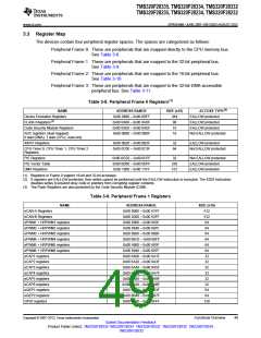
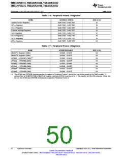
Table 3-10. Peripheral Frame 2 Registers
NAME
System Control Registers
ADDRESS RANGE
0x00 7010 – 0x00 702F
0x00 7040 – 0x00 704F
0x00 7050 – 0x00 705F
0x00 7070 – 0x00 707F
0x00 7100 – 0x00 711F
0x00 7750 – 0x00 775F
0x00 7770 – 0x00 777F
0x00 7900 – 0x00 793F
SIZE (x16)
32
16
16
16
32
16
16
64
SPI-A Registers
SCI-A Registers
External Interrupt Registers
ADC Registers
SCI-B Registers
SCI-C Registers
I2C-A Registers
Table 3-11. Peripheral Frame 3 Registers
NAME
ADDRESS RANGE
0x5000 – 0x503F
0x5040 – 0x507F
0x5800 – 0x583F
0x5840 – 0x587F
0x5880 – 0x58BF
0x58C0 – 0x58FF
0x5900 – 0x593F
0x5940 – 0x597F
SIZE (x16)
McBSP-A Registers (DMA)
McBSP-B Registers (DMA)
ePWM1 + HRPWM1 (DMA)(1)
ePWM2 + HRPWM2 (DMA)
ePWM3 + HRPWM3 (DMA)
ePWM4 + HRPWM4 (DMA)
ePWM5 + HRPWM5 (DMA)
ePWM6 + HRPWM6 (DMA)
64
64
64
64
64
64
64
64
(1) The ePWM and HRPWM modules can be re-mapped to Peripheral Frame 3 where they can be accessed by the DMA module. To
achieve this, bit 0 (MAPEPWM) of MAPCNF register (address 0x702E) must be set to 1. This register is EALLOW protected. When this
bit is 0, the ePWM and HRPWM modules are mapped to Peripheral Frame 1.
50
Functional Overview
Copyright © 2007–2012, Texas Instruments Incorporated
Submit Documentation Feedback
Product Folder Link(s): TMS320F28335 TMS320F28334 TMS320F28332 TMS320F28235 TMS320F28234
TMS320F28232

 TI [ TEXAS INSTRUMENTS ]