TMS320C6672
Multicore Fixed and Floating-Point Digital Signal Processor
SPRS708C—February 2012
www.ti.com
3 Device Configuration
On the TMS320C6672 device, certain device configurations like boot mode and endianess, are selected at device
power-on reset. The status of the peripherals (enabled/disabled) is determined after device power-on reset.
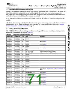
3.1 Device Configuration at Device Reset
Table 3-1 describes the device configuration pins. The logic level is latched at power-on reset to determine the device
configuration. The logic level on the device configuration pins can be set by using external pullup/pulldown resistors
or by using some control device (e.g., FPGA/CPLD) to intelligently drive these pins. When using a control device,
care should be taken to ensure there is no contention on the lines when the device is out of reset. The device
configuration pins are sampled during power-on reset and are driven after the reset is removed. To avoid
contention, the control device must stop driving the device configuration pins of the DSP. And when driving by a
control device, the control device must be fully powered and out of reset itself and driving the pins before the DSP
can be taken out of reset.
Also, please note that most of the device configuration pins are shared with other function pins
(LENDIAN/GPIO[0], BOOTMODE[12:0]/GPIO[13:1], PCIESSMODE[1:0]/GPIO[15:14] and PCIESSEN/TIMI0),
some time must be given following the rising edge of reset in order to drive these device configuration input pins
before they assume an output state (those GPIO pins should not become outputs during boot). Another caution that
needs to be noted is that systems using TIMI0 (pin shared with PCIESSEN) as a clock input must assure that the
clock itself is disabled from the input until after reset is released and a control device is no longer driving that input.
Note—If a configuration pin must be routed out from the device and it is not driven (Hi-Z state), the internal
pullup/pulldown (IPU/IPD) resistor should not be relied upon. TI recommends the use of an external
pullup/pulldown resistor. For more detailed information on pullup/pulldown resistors and situations in
which external pullup/pulldown resistors are required, see Section 3.4 ‘‘Pullup/Pulldown Resistors’’ on
page 90.
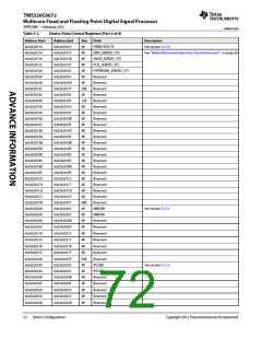
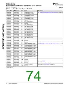
Table 3-1
TMS320C6672 Device Configuration Pins
(1)
Configuration Pin
Pin No.
IPD/IPU
Functional Description
LENDIAN(1) (2)
H25
IPU
Device endian mode (LENDIAN).
0 = Device operates in big endian mode
1 = Device operates in little endian mode
BOOTMODE[12:0] (1) (2)
PCIESSMODE[1:0] (1) (2)
J28, J29, J26, J25,
J27, J24, K27, K28,
K26, K29, L28, L29,
K25
IPD
IPD
Method of boot.
Some pins may not be used by bootloader and can be used as general purpose config
pins. Refer to the Bootloader for the C66x DSP User Guide in ‘‘Related Documentation from
Texas Instruments’’ on page 69 for how to determine the device enumeration ID value.
L27, K24
PCIe Subsystem mode selection.
00 = PCIe in end point mode
01 = PCIe legacy end point (support for legacy INTx)
10 = PCIe in root complex mode
11 = Reserved
PCIESSEN (1) (2)
PACLKSEL(1)
L24
AE4
IPD
IPD
PCIe subsystem enable/disable.
0 = PCIE Subsystem is disabled
1 = PCIE Subsystem is enabled
Network Coprocessor (PASS PLL) input clock select.
0 = CORECLK is used as the input to PASS PLL
1 = PASSCLK is used as the input to PASS PLL
End of Table 3-1
1 Internal 100-μA pulldown or pullup is provided for this terminal. In most systems, a 1-kΩ resistor can be used to oppose the IPD/IPU. For more detailed information on
pulldown/pullup resistors and situations in which external pulldown/pullup resistors are required, see Section 3.4 ‘‘Pullup/Pulldown Resistors’’ on page 90.
2 These signal names are the secondary functions of these pins.
70
Device Configuration
Copyright 2012 Texas Instruments Incorporated

 TI [ TEXAS INSTRUMENTS ]