TLV7103318-Q1
TLV7101828-Q1
SBVS202A –MARCH 2013–REVISED MARCH 2013
www.ti.com
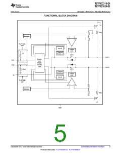
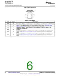
PIN CONFIGURATION
DSE PACKAGE
1.5mm x 1.5mm SON-6
(TOP VIEW)
EN1
IN
1
2
3
6
5
4
OUT1
OUT2
GND
EN2
PIN DESCRIPTIONS
NAME
PIN NO.
DESCRIPTION
Enable pin for regulator 1. Driving EN1 over 0.9V turns on regulator 1. Driving EN below 0.4V puts regulator
1 into shutdown mode.
EN1
1
Input pin. A small capacitor is needed from this pin to ground to assure stability. See Input and Output
Capacitor Requirements in the Application Information section for more details.
IN
2
Enable pin for regulator 2. Driving EN2 over 0.9V turns on regulator 2. Driving EN2 below 0.4V puts
regulator2 into shutdown mode.
EN2
3
4
GND
Ground pin.
Regulated output voltage pin. A small 1μF ceramic capacitor is needed from this pin to ground to assure
stability. See Input and Output Capacitor Requirements in the Application Information section for more
details.
OUT2
OUT1
5
6
Regulated output voltage pin. A small 1μF ceramic capacitor is needed from this pin to ground to assure
stability. See Input and Output Capacitor Requirements in the Application Information section for more
details.
6
Submit Documentation Feedback
Copyright © 2013, Texas Instruments Incorporated
Product Folder Links: TLV7103318-Q1 TLV7101828-Q1

 TI [ TEXAS INSTRUMENTS ]