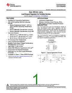
TLV7103318-Q1
TLV7101828-Q1
SBVS202A –MARCH 2013–REVISED MARCH 2013
www.ti.com
This integrated circuit can be damaged by ESD. Texas Instruments recommends that all integrated circuits be handled with
appropriate precautions. Failure to observe proper handling and installation procedures can cause damage.
ESD damage can range from subtle performance degradation to complete device failure. Precision integrated circuits may be more
susceptible to damage because very small parametric changes could cause the device not to meet its published specifications.
DEVICE DETAILS
(1)
PRODUCT
VOUT
TLV710xxyyqwwwz
XX is nominal output voltage of channel 1 (for example 18 = 1.8 V).
YY is nominal output voltage of channel 2 (for example 28 = 2.8V).
Q is optional. Use "U" for devices with EN pin pull-up resistor, and "D" for devices with EN
pin pull-down resistor.
WWW is package designator.
Z is package quantity. Use "R" for reel (3000 pieces), and "T" for tape (250 pieces).
(1) Output voltages from 1.2V to 4.8V in 50mV increments are available through the use of innovative factory OTP programming; minimum
order quantities may apply. Contact factory for details and availability.
ORDERING INFORMATION(1)
ORDERABLE PART NUMBER
TLV7103318QDSERQ1
TA
PACKAGE(2)
TOP-SIDE MARKING
ZD
CP
–40°C to 125°C
WSON-DSE Reel of 3000
TLV7101828QDSERQ1
(1) For the most-current package and ordering information, see the Package Option Addendum at the end of this document, or visit the
device product folder on www.ti.com.
(2) Package drawings, thermal data, and symbolization are available at www.ti.com/packaging.
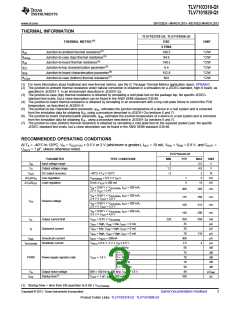
ABSOLUTE MAXIMUM RATINGS(1)
At TA = –40°C to 125°C (unless otherwise noted).
VALUE
MIN
–0.3
–0.3
–0.3
MAX
UNIT
V
IN
6
VIN 0.3
6
Voltage(2)
EN
V
OUT
OUT
V
Current
Internally limited
Indefinite
–40
A
Output short-circuit duration
s
Operating ambient, TA
125
150
150
2
°C
°C
°C
kV
Temperature
Junction, TJ
Storage, Tstg
–55
Human-Body Model (HBM) AEC-Q100 Classification Level H2
Electrostatic Discharge (ESD) rating
Charged-Device Model (CDM) AEC-Q100 Classification Level
C4B
750
V
(1) Stresses beyond those listed under Absolute Maximum Ratings may cause permanent damage to the device. These are stress ratings
only, and functional operation of the device at these or any other conditions beyond those indicated under Recommended Operating
Conditions is not implied. Exposure to absolute-maximum-rated conditions for extended periods my affect device reliability.
(2) All voltages with respect to ground.
2
Submit Documentation Feedback
Copyright © 2013, Texas Instruments Incorporated
Product Folder Links: TLV7103318-Q1 TLV7101828-Q1

 TI [ TEXAS INSTRUMENTS ]