TLV7103318-Q1
TLV7101828-Q1
www.ti.com
SBVS202A –MARCH 2013–REVISED MARCH 2013
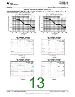
As with any linear regulator, PSRR and transient
response are degraded as (VIN – VOUT) approaches
dropout.
use worst-case loads and signal conditions. For good
reliability, thermal protection should trigger at least
35°C above the maximum expected ambient
condition of the particular application. This
configuration produces
temperature of 125°C at the highest expected
ambient temperature and worst-case load.
a
worst-case junction
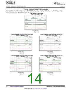
TRANSIENT RESPONSE
As with any regulator, increasing the size of the
output capacitor reduces over/undershoot magnitude
but increases duration of the transient response.
The internal protection circuitry of the TLV7103318-
Q1 and TLV7101828-Q1 has been designed to
protect against overload conditions. It was not
intended to replace proper heatsinking. Continuously
running the TLV710-Q1 into thermal shutdown
degrades device reliability.
The TLV7103318-Q1 and TLV7101828-Q1 each
have a dedicated VREF. Consequently, crosstalk from
one channel to the other as a result of transients is
close to 0V.
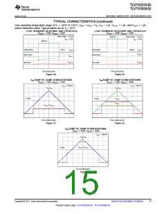
UNDERVOLTAGE LOCKOUT (UVLO)
POWER DISSIPATION
The TLV7103318-Q1and TLV7101828-Q1 use an
undervoltage lockout circuit to keep the output shut
off until the internal circuitry is operating properly.
The ability to remove heat from a die is different for
each
package
type,
presenting
different
considerations in the printed circuit board (PCB)
layout. The PCB area around the device that is free
of other components moves the heat from the device
to the ambient air.
THERMAL INFORMATION
Thermal protection disables the output when the
junction temperature rises to approximately 165°C,
allowing the device to cool. When the junction
temperature cools to approximately 145°C, the output
circuitry is again enabled. Depending on power
dissipation, thermal resistance, and ambient
temperature, the thermal protection circuit may cycle
on and off. This cycling limits the dissipation of the
regulator, protecting it from damage as a result of
overheating.
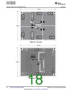
Performance data for the TLV710-Q1 evaluation
module (EVM) are shown in Table 1. The EVM is a 2-
layer board with 2 ounces of copper per side. The
dimension and layout are shown in Figure 54 and
Figure 55. Using heavier copper increases the
effectiveness of removing heat from the device. The
addition of plated through-holes in the heat-
dissipating layer also improves the heatsink
effectiveness. Power dissipation depends on input
voltage and load conditions.
Any tendency to activate the thermal protection circuit
indicates excessive power dissipation or an
inadequate heatsink. For reliable operation, junction
temperature should be limited to 125°C maximum. To
estimate the margin of safety in a complete design
Power dissipation (PD) is equal to the product of the
output current and the voltage drop across the output
pass element, as shown in Equation 1:
PD = (VIN – VOUT) × IOUT
(1)
(including
heatsink),
increase
the
ambient
temperature until the thermal protection is triggered;
PACKAGE MOUNTING
Solder pad footprint recommendations for the
TLV7103318-Q1 and TLV7101828-Q1 are available
from the Texas Instruments Web site at www.ti.com.
The recommended land pattern for the DSE (SON-6)
package is shown in .
Table 1. TLV7103318-Q1 and TLV7101828-Q1 EVM Dissipation Ratings
PACKAGE
RθJA
170°C/W
TA < 25°C
585 mW
TA = 85°C
235 mW
TA = 125°C
DSE
mW
Copyright © 2013, Texas Instruments Incorporated
Submit Documentation Feedback
17
Product Folder Links: TLV7103318-Q1 TLV7101828-Q1

 TI [ TEXAS INSTRUMENTS ]