TLV7103318-Q1
TLV7101828-Q1
SBVS202A –MARCH 2013–REVISED MARCH 2013
www.ti.com
APPLICATION INFORMATION
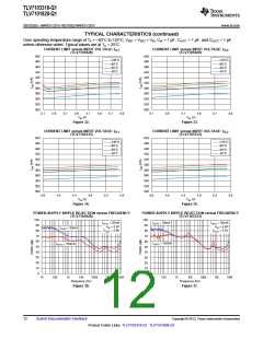
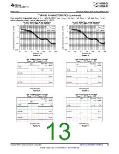
IMPROVE PSRR AND NOISE PERFORMANCE
The TLV7103318-Q1 and TLV7101828-Q1 devices
belong to a new family of next-generation, value LDO
regulators. These devices consume low quiescent
current and deliver excellent line and load transient
performance. These features, combined with low
Input and output capacitors should be placed as
close to the device pins as possible. To improve ac
performance such as PSRR, output noise, and
transient response, it is recommended that the board
be designed with separate ground planes for VIN and
VOUT, with the ground plane connected only at the
GND pin of the device. In addition, the ground
connection for the output capacitor should be
connected directly to the GND pin of the device. High
ESR capacitors may degrade PSRR.
noise, very good PSRR with little (VIN to VOUT
)
headroom, make these devices ideal for RF portable
applications. This family of LDO regulators offers
current limit and thermal protection, and is specified
from –40°C to 125°C.
INPUT AND OUTPUT CAPACITOR
REQUIREMENTS
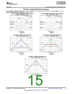
INTERNAL CURRENT LIMIT
1.0μF X5R- and X7R-type ceramic capacitors are
recommended because they have minimal variation
in value and equivalent series resistance (ESR) over
temperature.
The TLV7103318-Q1 and TLV7101828-Q1 internal
current limits help protect the regulator during fault
conditions. During current limit, the output sources a
fixed amount of current that is largely independent of
output voltage. In such a case, the output voltage is
However, the TLV7103318-Q1 and TLV7101828-Q1
are designed to be stable with an effective
capacitance of 0.1 μF or larger at the output. Thus,
the device would also be stable with capacitors of
other dielectrics, as long as the effective capacitance
under operating bias voltage and temperature is
greater than 0.1 μF. This effective capacitance refers
to the capacitance that the device sees under
operating bias voltage and temperature conditions
(that is, the capacitance after taking bias voltage and
temperature derating into consideration.)
not regulated, and is VOUT = ILIMIT × RLOAD
.
The PMOS pass transistor dissipates (VIN – VOUT) ×
ILIMIT until thermal shutdown is triggered and the
device is turned off. As the device cools down, it is
turned on by the internal thermal shutdown circuit. If
the fault condition continues, the device cycles
between current limit and thermal shutdown. See the
Thermal Information section for more details. The
PMOS pass element in the TLV7103318-Q1 and
TLV7101828-Q1 has a built-in body diode that
conducts current when the voltage at OUT exceeds
the voltage at IN. This current is not limited, so if
extended reverse voltage operation is anticipated,
external limiting to 5% of rated output current is
recommended.
In addition to allowing the use of cost-effective
dielectrics, these devices also enable using smaller
footprint capacitors that have a higher derating in
size-constrained applications.
Note that using a 0.1-μF rating capacitor at the output
of the LDO regulator does not ensure stability
because the effective capacitance under operating
conditions would be less than 0.1 μF. The maximum
ESR should be less than 200 mΩ.
SHUTDOWN
The enable pin (EN) is active high. The device is
enabled when EN pin goes above 0.9V. This
relatively lower value of voltage needed to turn the
LDO regulator on can be used to enable the device
with the GPIO of recent processors whose GPIO
voltage is lower than traditional microcontrollers.
Although an input capacitor is not required for
stability, it is good analog design practice to connect
a 0.1μF to 1.0μF low ESR capacitor across the IN
and GND pins of the regulator. This capacitor
counteracts reactive input sources and improves
transient response, noise rejection, and ripple
rejection. A higher-value capacitor may be necessary
if large, fast-rise-time load transients are anticipated,
or if the device is not located near the power source.
If source impedance is more than 2Ω, a 0.1μF input
capacitor may be necessary to ensure stability.
The device is turned off when the EN pin is held at
less than 0.4 V. When shutdown capability is not
required, the EN pin can be connected to the IN pin.
DROPOUT VOLTAGE
The TLV7103318-Q1 and TLV7101828-Q1 use a
PMOS pass transistor to achieve low dropout. When
(VIN – VOUT) is less than the dropout voltage (VDO),
the PMOS pass device is in the linear region of
operation and the input-to-output resistance is the
RDS(ON) of the PMOS pass element. VDO scales
approximately with the output current because the
PMOS device behaves as a resistor in dropout.
BOARD LAYOUT RECOMMENDATIONS TO
16
Submit Documentation Feedback
Copyright © 2013, Texas Instruments Incorporated
Product Folder Links: TLV7103318-Q1 TLV7101828-Q1

 TI [ TEXAS INSTRUMENTS ]