Circuit Description
In larger computers several features are provided to prevent such errors: a power-fail interrupt signals
dangerous conditions in time, the content of the memory is protected by a battery back-up, and so on. In
small microcomputer systems this amount of effort is too expensive, and in most applications also not
required. It is usually sufficient if, after a serious voltage drop, the microcomputer is forced into a defined
initial condition. To implement this function, whilst preventing the problems mentioned above, the following
circuit features are required:
- Accurate detection of a serious voltage drop.
- Generation of a reset signal while as the supply voltage is not in the operational
range, to prevent undefined operations of the microcomputer.
- Maintenance of the reset signal for a certain time after the supply voltage has
returned to its nominal value, to ensure proper initialization of the circuit.
For these applications, Texas Instruments has developed a series of integrated circuits which, with a
minimum of external components and without additional adjustment, will fulfill the requirements described
above.
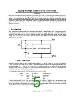
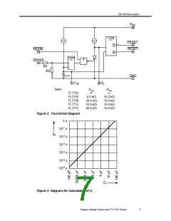
2. Circuit Description
The main part of this circuit is a reference voltage source, which consists of a very stable, temperature-
compensated band gap reference. An external capacitor (typ. 0.1mF) must be connected to the voltage
output Vref, to reduce the influence of fast transients in the supply voltage. The voltage at the SENSE input
is divided by a resistor divider and compared with the reference voltage by a comparator. To achieve high
accuracy, this divider is adjusted at wafer probe. When the input voltage is sensed to be lower than the
threshold voltage, the thyristor is triggered, which discharges the timing capacitor C. It is also possible to
t
fire the thyristor via the RESIN input by a logic level (TTL level, active low). The thyristor is turned off again
when either the voltage at the SENSE input (orRESIN input) increases beyond the threshold, or - during
short supply voltage drops - the discharge current of the capacitor becomes lower than the hold current of
the thyristor.
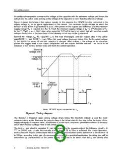
Thereafter, the capacitor is recharged by a current source 100mA, the charge time being calculated as
follows:
td = 1.3×10⁴ ×Ct
Ct in F, t in s
The magnitude of charge current and therefore also the delay dt time is determined by the tolerance of the
resistors in the integrated circuit. These tolerances, caused by the semiconductor manufacturing process,
are not negligible. Therefore the delay time may vary -50% to +100 %. However, for the applications
discussed here this will not be a restriction. The diagram in figure 3 shows the typical delay time dt versus
the capacitance of the external capacitor C.
t
2
Literature Number: SLVAE04

 TI [ TEXAS INSTRUMENTS ]