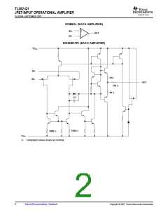
TL082-Q1
JFET-INPUT OPERATIONAL AMPLIFIER
www.ti.com
SLOS548–SEPTEMBER 2007
ELECTRICAL CHARACTERISTICS(1)
VCC± = ±15 V (unless otherwise noted)
(2)
PARAMETER
TEST CONDITIONS
TA
MIN
TYP
MAX UNIT
25°C
3
6
VIO
αVIO
IIO
Input offset voltage
VO = 0, RS = 50 Ω
VO = 0, RS = 50 Ω
VO = 0
mV
9
Full range
Temperature coefficient of input
offset voltage
Full range
18
5
μV/°C
25°C
Full range
25°C
100
20
pA
nA
pA
nA
Input offset current(3)
Input bias current(3)
30
200
50
IIB
VO = 0
Full range
Common-mode input
voltage range
–12
to 15
VICR
25°C
25°C
±11
V
RL = 10 kΩ
±12 ±13.5
±12
Maximum peak output
voltage swing
VOM
R
L ≥ 10 kΩ
L ≥ 2 kΩ
V
Full range
R
±10
50
±12
200
25°C
Full range
25°C
Large-signal differential voltage
amplification
AVD
VO = ±10 V, RL ≥ 2 kΩ
V/mV
15
B1
Unity-gain bandwidth
3
1012
86
MHz
Ω
ri
Input resistance
25°C
CMRR
Common-mode rejection ratio
VIC = VICR(min), VO = 0, RS = 50 Ω
25°C
75
80
dB
Supply-voltage rejection ratio
VCC = ±15 V to ±9 V,
VO = 0, RS = 50 Ω
kSVR
25°C
86
dB
(ΔVCC±/ΔVIO
)
ICC
Supply current (per amplifier)
Crosstalk attenuation
VO = 0, No load
AVD = 100
25°C
25°C
1.4
2.8
mA
dB
VO1/VO2
120
(1) All characteristics are measured under open-loop conditions with zero common-mode voltage, unless otherwise specified.
(2) Full range for TA is –40°C to 85°C for I-suffix devices and –40°C to 125°C for Q-suffix devices.
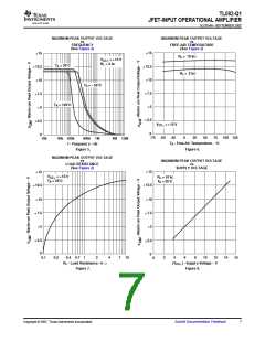
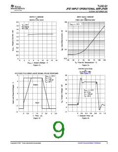
(3) Input bias currents of an FET-input operational amplifier are normal junction reverse currents, which are temperature sensitive, as
shown in Figure 14. Pulse techniques must be used that maintain the junction temperature as close to the ambient temperature as
possible.
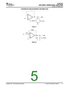
OPERATING CHARACTERISTICS
VCC± = ±15 V, TA = 25°C (unless otherwise noted)
PARAMETER
Slew rate at unity gain
Rise time
TEST CONDITIONS
MIN
TYP
13
MAX
UNIT
V/μs
μs
SR
tr
VI = 10 V, RL = 2 kΩ, CL = 100 pF, See Figure 1
VI = 20 mV, RL = 2 kΩ, CL = 100 pF, See Figure 1
VI = 20 mV, RL = 2 kΩ, CL = 100 pF, See Figure 1
8
0.05
20
Overshoot factor
%
f = 1 kHz
RS = 20 Ω
18
nV/√Hz
μV
Vn
Equivalent input noise voltage
f = 10 Hz to 10 kHz
4
In
Equivalent input noise current
Total harmonic distortion
RS = 20 Ω, f = 1 kHz
0.01
0.003
pA/√Hz
%
THD
VIrms = 6 V, f = 1 kHz, AVD = 1, RS ≤ 1 kΩ, RL ≥ 2 kΩ
4
Submit Documentation Feedback
Copyright © 2007, Texas Instruments Incorporated

 TI [ TEXAS INSTRUMENTS ]