TL081M, TL082M, TL084M
JFET-INPUT OPERATIONAL AMPLIFIERS
SLOS081A–D2297, FEBRUARY 1977–REVISED NOVEMBER 1992
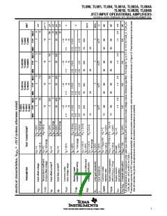
electrical characteristics, V
= ±15 V (unless otherwise noted)
CC ±
TL081M, TL082M
TL084M
TYP
3
†
PARAMETER
TEST CONDITIONS
UNIT
MIN
TYP
MAX
MIN
MAX
9
T
= 25°C
3
6
9
A
V
IO
Input offset voltage
V
V
= 0,
= 0,
R = 50 Ω
S
mV
O
T
A
= –55°C to 125°C
15
Temperature
coefficient of input
offset voltage
R = 50 Ω,
O
S
α
18
5
18
5
µV/°C
VIO
T
A
= –55°C to 125°C
T
A
T
A
T
A
T
A
= 25°C
= 125°C
= 25°C
= 125°C
100
20
100
20
pA
nA
pA
nA
‡
I
I
Input offset current
V
= 0
= 0
IO
O
O
30
200
50
30
200
50
‡
Input bias current
Common-mode
V
IB
± 12
± 12
to
15
to
V
T
A
= 25°C
±11
±11
V
V
ICR
OM
input voltage range
15
T
A
= 25°C,
R
R
R
R
= 10 kΩ
≥ 10 kΩ
≥ 2 kΩ
±12 ±13.5
±12
±12 ±13.5
±12
Maximum peak
output voltage
swing
L
L
L
L
V
T
A
= –55°C to 125°C
±10
±12
±10
±12
V
T
A
= ±10 V,
= 25°C
≥ 2 kΩ,
O
25
200
25
200
Large-signal
differential voltage
amplification
A
VD
V/mV
V
T
A
= ±10 V,
= –55°C to 125°C
R
≥ 2 kΩ,
O
L
15
15
Unity-gain
bandwidth
B
T
= 25°C
= 25°C
A
3
3
MHz
Ω
1
A
12
12
r
i
Input resistance
T
10
10
Common-mode
rejection ratio
V
R
= V
= 50 Ω,
min,
V
T
A
= 0,
= 25°C
IC
S
ICR
O
CMRR
80
80
86
80
80
86
dB
Supply voltage
rejection ratio
V
R
= ±15 V to ±9 V,
= 50 Ω,
V
T
A
= 0,
= 25°C
CC
O
k
86
86
dB
SVR
S
(∆V
CC±
/∆V )
IO
Supply current
(per amplifier)
I
No load,
= 100,
V
= 0,
T
= 25°C
1.4
2.8
1.4
2.8
mA
dB
CC
O
A
Crosstalk
attenuation
V
/V
A
T
A
= 25°C
120
120
01 02
VD
†
‡
All characteristics are measured under open-loop conditions with zero common-mode input voltage unless otherwise specified.
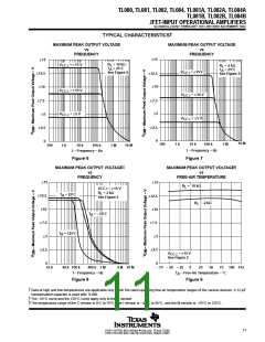
Input bias currents of a FET-input operational amplifier are normal junction reverse currents, which are temperature sensitive as shown in
Figure 18. Pulse techniques must be used that will maintain the junction temperatures as close to the ambient temperature as is possible.
operating characteristics, V
= ±15 V, T = 25°C (unless otherwise noted)
A
CC±
PARAMETER
TEST CONDITIONS
MIN
TYP MAX
UNIT
V/µs
µs
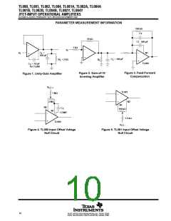
V = 10 V,
R
L
= 2 kΩ,
See Figure 1
I
8
13
C
= 100 pF,
L
SR
Slew rate at unity gain
V = 10 V,
R
= 2 kΩ,
C = 100 pF,
L
See Figure 1
I
A
L
5
T
= – 55°C to 125°C,
t
r
Rise time
V = 20 mV,
I
R = 2 kΩ,
L
See Figure 1
0.05
20%
18
Overshoot factor
C
R
R
= 100 pF,
= 100 Ω
= 100 Ω,
L
f = 1 kHz
nV/√Hz
µV
V
n
Equivalent input noise voltage
Equivalent input noise current
S
S
f = 10 Hz to 10 kHz
f = 1 kHz
4
I
n
0.01
pA/√Hz
V
= 10 V,
R
≤ 1 kΩ,
R ≥ 2 kΩ,
L
O(rms)
f = 1 kHz
S
THD Total harmonic distortion
0.003%
On products compliant to MIL-STD-883, Class B, this parameter is not production tested.
8
POST OFFICE BOX 655303 • DALLAS, TEXAS 75265
POST OFFICE BOX 1443 • HOUSTON, TEXAS 77001

 TI [ TEXAS INSTRUMENTS ]