THS4531
SLOS358B –SEPTEMBER 2011–REVISED MARCH 2012
www.ti.com
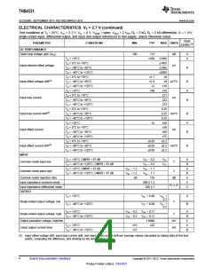
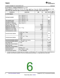
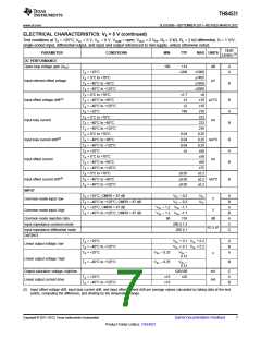
ELECTRICAL CHARACTERISTICS: VS = 5 V (continued)
Test conditions at TA = +25°C, VS+ = 5 V, VS– = 0 V, VOCM = open, VOUT = 2 VPP, RF = 2 kΩ, RL = 2 kΩ differential, G = 1 V/V,
single-ended input, differential output, and input and output referenced to mid-supply, unless otherwise noted.
TEST
LEVEL(1)
PARAMETER
CONDITIONS
MIN
TYP
MAX UNITS
POWER SUPPLY
Specified operating voltage
2.5
5.5
350
390
V
B
A
B
A
TA = 25°C, PD = VS+
250
290
108
Quiescent operating current/ch
µA
dB
TA = –40°C to 125°C, PD = VS+
Power-supply rejection (±PSRR)
POWER DOWN
87
Enable voltage threshold
Disable voltage threshold
Disable pin bias current
Power-down quiescent current
Turn-on time delay
Specified on above 2.1 V
Specified off below 0.7 V
PD = VS– + 0.5 V
2.1
A
A
A
A
V
0.7
50
0.5
500
2
nA
µA
PD = VS– + 0.5 V
Time from PD = high to VOUT = 90% of final
600
value, RL= 200 Ω
ns
C
Time from PD = low to VOUT = 10% of
original value, RL= 200 Ω
Turn-off time delay
15
OUTPUT COMMON-MODE VOLTAGE CONTROL (VOCM
)
Small-signal bandwidth
Slew rate
VOCM input = 100 mVPP
24
15
MHz
V/µs
V/V
C
C
A
A
VOCM input = 1 VSTEP
Gain
0.99
0.95
0.996
±1
1.01
±5
Common-mode offset voltage
Offset = output common-mode voltage –
VOCM input voltage
mV
VOCM input bias current
VOCM input voltage range
VOCM = (VS+ – VS–)/2
±20
±120
4.0
nA
V
A
A
0.75 to
4.15
VOCM input impedance
65 || 0.86
±3
kΩ || pF
C
A
Default voltage offset from
(VS+ – VS–)/2
Offset = output common-mode voltage –
(VS+ – VS–)/2
±10
mV
8
Submit Documentation Feedback
Copyright © 2011–2012, Texas Instruments Incorporated
Product Folder Link(s): THS4531

 TI [ TEXAS INSTRUMENTS ]