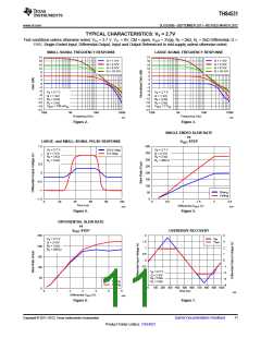
THS4531
www.ti.com
SLOS358B –SEPTEMBER 2011–REVISED MARCH 2012
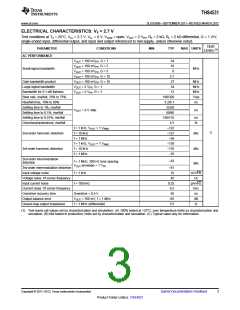
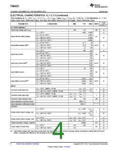
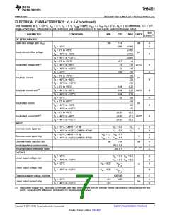
ELECTRICAL CHARACTERISTICS: VS = 5 V (continued)
Test conditions at TA = +25°C, VS+ = 5 V, VS– = 0 V, VOCM = open, VOUT = 2 VPP, RF = 2 kΩ, RL = 2 kΩ differential, G = 1 V/V,
single-ended input, differential output, and input and output referenced to mid-supply, unless otherwise noted.
TEST
LEVEL(1)
PARAMETER
CONDITIONS
MIN
TYP
MAX UNITS
DC PERFORMANCE
Open-loop voltage gain (AOL
)
100
114
dB
A
A
TA = +25°C
±200
±1000
TA = 0°C to +70°C
TA = –40°C to +85°C
TA = –40°C to +125°C
TA = 0°C to +70°C
TA = –40°C to +85°C
TA = –40°C to +125°C
TA = +25°C
±1405
µV
Input-referred offset voltage
±1650
B
±2000
±9
±1.7
±2
Input offset voltage drift(2)
Input bias current
±10 µV/°C
±10
B
A
B
±2
160
210
TA = 0°C to +70°C
TA = –40°C to +85°C
TA = –40°C to +125°C
TA = 0°C to +70°C
TA = –40°C to +85°C
TA = –40°C to +125°C
TA = +25°C
222
nA
223
235
0.04
0.04
0.04
±5
0.25
Input bias current drift(2)
Input offset current
0.25 nA/°C
0.25
B
A
B
±50
TA = 0°C to +70°C
TA = –40°C to +85°C
TA = –40°C to +125°C
TA = 0°C to +70°C
TA = –40°C to +85°C
TA = –40°C to +125°C
±59
nA
±60
±75
±0.05
±0.05
±0.05
±0.2
Input offset current drift(2)
±0.2 nA/°C
±0.2
B
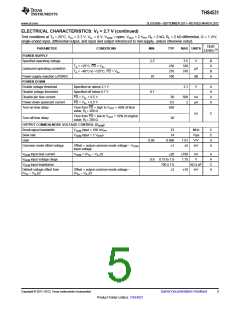
INPUT
TA = +25°C, CMRR > 87 dB
VS– – 0.2
VS– – 0.2
VS–
A
B
A
B
A
C
C
Common-mode input: low
V
TA = –40°C to +125°C, CMRR > 87 dB
TA = +25°C, CMRR > 87 dB
VS–
VS+ – 1.2 VS+ –1.1
VS+ – 1.2 VS+ –1.1
Common-mode input: high
V
dB
TA = –40°C to +125°C, CMRR > 87 dB
Common-mode rejection ratio
Input impedance common-mode
Input impedance differential mode
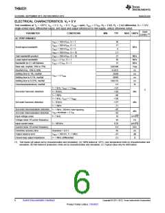
OUTPUT
90
116
200 || 1.2
200 || 1
kΩ || pF
TA = +25°C
VS– + 0.1 VS– + 0.2
VS– + 0.1 VS– + 0.2
A
B
A
Linear output voltage: low
TA = –40°C to +125°C
TA = +25°C
VS+ – 0.25
VS+ – 0.25
VS+
–
V
0.12
Linear output voltage: high
TA = –40°C to +125°C
VS+
–
B
0.12
Output saturation voltage: high/low
Linear output current drive
120/100
±25
mV
mA
C
A
B
TA = +25°C
±15
±15
TA = –40°C to +125°C
(2) Input offset voltage drift, input bias current drift, and input offset current drift are average values calculated by taking data at the end
points, computing the difference, and dividing by the temperature range.
Copyright © 2011–2012, Texas Instruments Incorporated
Submit Documentation Feedback
7
Product Folder Link(s): THS4531

 TI [ TEXAS INSTRUMENTS ]