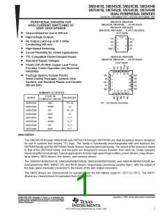
SN55451B, SN55452B, SN55453B, SN55454B
SN75451B, SN75452B, SN75453B, SN75454B
DUAL PERIPHERAL DRIVERS
SLRS021B – DECEMBER 1976 – REVISED SEPTEMBER 1999
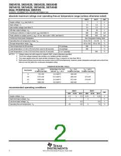
absolute maximum ratings over operating free-air temperature range (unless otherwise noted)
SN55’
7
SN75’
7
UNIT
V
Supply voltage, V
CC
(see Note 1)
Input voltage, V
5.5
5.5
30
5.5
5.5
30
V
I
Inter-emitter voltage (see Note 2)
Off-state output voltage, V
V
V
O
Continuous collector or output current, I
OK
(see Note 3)
400
500
400
500
mA
mA
Peak collector or output current, I (t ≤ 10 ms, duty cycle ≤ 50%, see Note 4)
I
w
Continuous total power dissipation
See Dissipation Rating Table
Operating free-air temperature range, T
–55 to 125
0 to 70
°C
°C
°C
°C
°C
A
Storage temperature range, T
stg
–65 to 150 –65 to 150
Case temperature for 60 seconds
FK package
JG package
D or P package
260
300
260
Lead temperature 1,6 mm (1/16 inch) from case for 60 seconds
Lead temperature 1,6 mm (1/16 inch) from case for 10 seconds
NOTES: 1. Voltage values are with respect to network GND, unless otherwise specified.
2. This is the voltage between two emitters of a multiple-emitter transistor.
3. This value applies when the base-emitter resistance (R ) is equal to or less than 500 Ω.
BE
4. Both halves of these dual circuits may conduct rated current simultaneously; however, power dissipation averaged over a short time
interval must fall within the continuous dissipation rating.
DISSIPATION RATING TABLE
T
≤ 25°C
DERATING FACTOR
T
= 70°C
T = 125°C
A
A
A
PACKAGE
POWER RATING
ABOVE T = 25°C
POWER RATING POWER RATING
A
D
FK
JG
P
725 mW
5.8 mW/°C
11.0 mW/°C
8.4 mW/°C
8.0 mW/°C
464 mW
880 mW
672 mW
640 mW
—
1375 mW
275 mW
210 mW
—
1050 mW
1000 mW
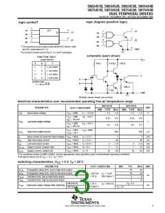
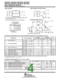
recommended operating conditions
SN55’
SN75’
MIN NOM
UNIT
MIN NOM
MAX
MAX
Supply voltage, V
CC
4.5
2
5
5.5
4.75
2
5
5.25
V
V
High-level input voltage, V
IH
Low-level input voltage, V
0.8
0.8
70
V
IL
Operating free-air temperature, T
–55
125
0
°C
A
2
POST OFFICE BOX 655303 • DALLAS, TEXAS 75265

 TI [ TEXAS INSTRUMENTS ]