SN74LVC1T45-Q1
SCES677A –SEPTEMBER 2006–REVISED AUGUST 2009 .......................................................................................................................................... www.ti.com
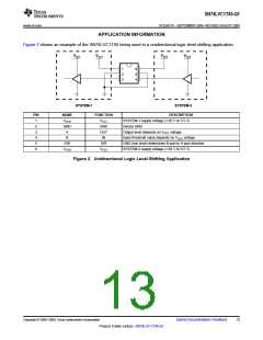
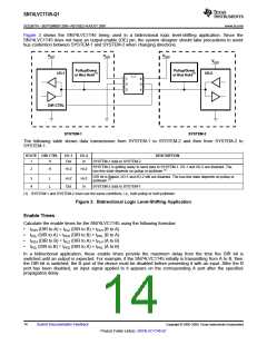
Figure 3 shows the SN74LVC1T45 being used in a bidirectional logic level-shifting application. Since the
SN74LVC1T45 does not have an output-enable (OE) pin, the system designer should take precautions to avoid
bus contention between SYSTEM-1 and SYSTEM-2 when changing directions.
VCC1
VCC1
VCC2
VCC2
Pullup/Down
or Bus Hold(1)
Pullup/Down
or Bus Hold(1)
I/O-1
I/O-2
1
2
3
6
5
4
DIR CTRL
SYSTEM-1
SYSTEM-2
The following table shows data transmission from SYSTEM-1 to SYSTEM-2 and then from SYSTEM-2 to
SYSTEM-1.
STATE DIR CTRL
I/O-1
I/O-2
DESCRIPTION
1
H
Out
In
SYSTEM-1 data to SYSTEM-2
SYSTEM-2 is getting ready to send data to SYSTEM-1. I/O-1 and I/O-2 are disabled. The
bus-line state depends on pullup or pulldown.(1)
2
H
Hi-Z
Hi-Z
DIR bit is flipped. I/O-1 and I/O-2 still are disabled. The bus-line state depends on pullup or
pulldown.(1)
3
4
L
L
Hi-Z
Out
Hi-Z
In
SYSTEM-2 data to SYSTEM-1
(1) SYSTEM-1 and SYSTEM-2 must use the same conditions, i.e., both pullup or both pulldown.
Figure 3. Bidirectional Logic Level-Shifting Application
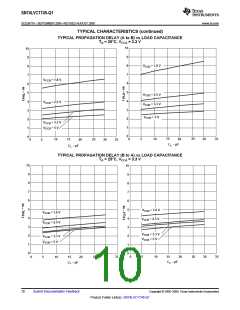
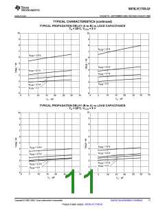
Enable Times
Calculate the enable times for the SN74LVC1T45 using the following formulas:
•
•
•
•
tPZH (DIR to A) = tPLZ (DIR to B) + tPLH (B to A)
tPZL (DIR to A) = tPHZ (DIR to B) + tPHL (B to A)
tPZH (DIR to B) = tPLZ (DIR to A) + tPLH (A to B)
tPZL (DIR to B) = tPHZ (DIR to A) + tPHL (A to B)
In a bidirectional application, these enable times provide the maximum delay from the time the DIR bit is
switched until an output is expected. For example, if the SN74LVC1T45 initially is transmitting from A to B, then
the DIR bit is switched; the B port of the device must be disabled before presenting it with an input. After the B
port has been disabled, an input signal applied to it appears on the corresponding A port after the specified
propagation delay.
14
Submit Documentation Feedback
Copyright © 2006–2009, Texas Instruments Incorporated
Product Folder Link(s): SN74LVC1T45-Q1

 TI [ TEXAS INSTRUMENTS ]