SN74LVC1T45-Q1
SCES677A –SEPTEMBER 2006–REVISED AUGUST 2009 .......................................................................................................................................... www.ti.com
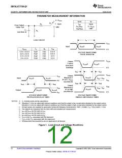
PARAMETER MEASUREMENT INFORMATION
2 × V
CCO
TEST
S1
S1
R
L
Open
GND
t
Open
pd
From Output
Under Test
t
t
/t
/t
2 × V
CCO
GND
PLZ PZL
PHZ PZH
C
L
R
L
(see Note A)
t
w
LOAD CIRCUIT
V
CCI
V
CCI
/2
V
CCI
/2
Input
C
L
V
TP
R
L
V
CCO
0 V
1.8 V ± 0.15 V
2.5 V ± 0.2 V
3.3 V ± 0.3 V
5 V ± 0.5 V
2 kΩ
2 kΩ
2 kΩ
2 kΩ
0.15 V
0.15 V
0.3 V
15 pF
15 pF
15 pF
15 pF
VOLTAGE WAVEFORMS
PULSE DURATION
0.3 V
V
CCA
Output
Control
(low-level
enabling)
V /2
CCA
V
CCA
/2
t
0 V
t
PZL
PLZ
V
V
CCO
Output
Waveform 1
V
CCI
V
/2
/2
CCO
Input
V
CCI
/2
V
CCI
/2
V
+ V
OL
TP
S1 at 2 × V
CCO
OL
0 V
(see Note B)
t
t
PZH
PHZ
t
t
PHL
PLH
Output
Waveform 2
S1 at GND
V
OH
V
OH
V
OH
− V
TP
V
CCO
Output
V /2
CCO
V
CCO
/2
(see Note B)
0 V
V
OL
VOLTAGE WAVEFORMS
PROPAGATION DELAY TIMES
VOLTAGE WAVEFORMS
ENABLE AND DISABLE TIMES
NOTES: A. C includes probe and jig capacitance.
L
B. Waveform 1 is for an output with internal conditions such that the output is low, except when disabled by the output control.
Waveform 2 is for an output with internal conditions such that the output is high, except when disabled by the output control.
C. All input pulses are supplied by generators having the following characteristics: PRR v10 MHz, Z = 50 Ω, dv/dt ≥ 1 V/ns.
O
D. The outputs are measured one at a time, with one transition per measurement.
E.
F.
G.
H.
I.
t
t
t
V
V
and t
and t
and t
are the same as t
.
dis
.
PLZ
PZL
PLH
PHZ
are the same as t
PZH
en
are the same as t .
pd
PHL
is the V associated with the input port.
CC
CCI
is the V associated with the output port.
CCO
CC
J. All parameters and waveforms are not applicable to all devices.
Figure 1. Load Circuit and Voltage Waveforms
12
Submit Documentation Feedback
Copyright © 2006–2009, Texas Instruments Incorporated
Product Folder Link(s): SN74LVC1T45-Q1

 TI [ TEXAS INSTRUMENTS ]