Introduction
2
Introduction
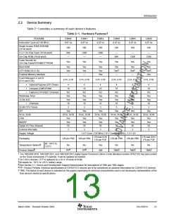
This section provides a summary of each device’s features, lists the pin assignments, and describes the
function of each pin. This document also provides detailed descriptions of peripherals, electrical
specifications, parameter measurement information, and mechanical data about the available packaging.
2.1
Description
The SM320F2810-EP, SM320F2811-EP, SM320F2812-EP, SM320C2810-EP, SM320C2811-EP, and
SM320C2812-EP devices, members of the TMS320C28x DSP generation, are highly integrated,
high-performance solutions for demanding control applications. The functional blocks and the memory maps
are described in Section 3, Functional Overview.
Throughout this document, SM320F2810-EP, SM320F2811-EP, and SM320F2812-EP are abbreviated as
F2810, F2811, and F2812, respectively. F281x denotes all three Flash devices. SM320C2810-EP,
SM320C2811-EP, and SM320C2812-EP are abbreviated as C2810, C2811, and C2812, respectively. C281x
denotes all three ROM devices. 2810 denotes both F2810 and C2810 devices; 2811 denotes both F2811 and
C2811 devices; and 2812 denotes both F2812 and C2812 devices.
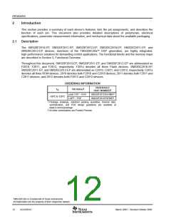
ORDERING INFORMATION
ORDERABLE
PART NUMBER
†
PACKAGE
T
A
‡
µstar CSP − GHH
SM320F2812GHHMEP
SM320F2812PGFMEP
−55°C to 125°C
LQFP − PGF
†
‡
Package drawings, standard packing quantities, thermal data,
symbolization, and PCB design guidelines are available at
www.ti.com/sc/package.
All other combinations are Product Preview.
TMS320C28x is a trademark of Texas Instruments.
All trademarks are the property of their respective owners.
12
SGUS051A
March 2004 − Revised October 2004

 TI [ TEXAS INSTRUMENTS ]