RM46L450
RM46L850
SPNS184 –SEPTEMBER 2012
www.ti.com
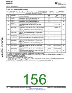
5.11.4 MibSPI/SPI Master Mode I/O Timing Specifications
Table 5-32. SPI Master Mode External Timing Parameters (CLOCK PHASE = 0, SPICLK = output, SPISIMO
= output, and SPISOMI = input)(1)(2)(3)
NO. Parameter
tc(SPC)M
2(5) tw(SPCH)M
MIN
4040
MAX
Unit
ns
1
Cycle time, SPICLK(4)
256tc(VCLK)
0.5tc(SPC)M + 3
Pulse duration, SPICLK high (clock
polarity = 0)
0.5tc(SPC)M – tr(SPC)M – 3
ns
tw(SPCL)M
3(5) tw(SPCL)M
tw(SPCH)M
Pulse duration, SPICLK low (clock
polarity = 1)
0.5tc(SPC)M – tf(SPC)M – 3
0.5tc(SPC)M – tf(SPC)M – 3
0.5tc(SPC)M – tr(SPC)M – 3
0.5tc(SPC)M – 5
0.5tc(SPC)M + 3
0.5tc(SPC)M + 3
0.5tc(SPC)M + 3
Pulse duration, SPICLK low (clock
polarity = 0)
ns
ns
ns
ns
ns
ns
ns
Pulse duration, SPICLK high (clock
polarity = 1)
4(5) td(SPCH-SIMO)M Delay time, SPISIMO valid before
SPICLK low (clock polarity = 0)
td(SPCL-SIMO)M Delay time, SPISIMO valid before
SPICLK high (clock polarity = 1)
5(5) tv(SPCL-SIMO)M
0.5tc(SPC)M – 5
Valid time, SPISIMO data valid after
SPICLK low (clock polarity = 0)
0.5tc(SPC)M – tf(SPC) – 3
0.5tc(SPC)M – tr(SPC) – 3
0.5tf(SPC) + 2
tv(SPCH-SIMO)M Valid time, SPISIMO data valid after
SPICLK high (clock polarity = 1)
6(5) tsu(SOMI-SPCL)M Setup time, SPISOMI before SPICLK
low (clock polarity = 0)
tsu(SOMI-SPCH)M Setup time, SPISOMI before SPICLK
high (clock polarity = 1)
7(5) th(SPCL-SOMI)M Hold time, SPISOMI data valid after
SPICLK low (clock polarity = 0)
0.5tf(SPC) + 2
5
th(SPCH-SOMI)M Hold time, SPISOMI data valid after
SPICLK high (clock polarity = 1)
8(6) tC2TDELAY
5
Setup time CS active
until SPICLK high
(clock polarity = 0)
CSHOLD = 0 C2TDELAY*tc(VCLK) + 2*tc(VCLK)
- tf(SPICS) + tr(SPC) – 15
(C2TDELAY+2) * tc(VCLK)
tf(SPICS) + tr(SPC) + 3
-
-
-
-
CSHOLD = 1 C2TDELAY*tc(VCLK) + 3*tc(VCLK)
- tf(SPICS) + tr(SPC) – 15
(C2TDELAY+3) * tc(VCLK)
tf(SPICS) + tr(SPC) + 3
Setup time CS active
until SPICLK low
CSHOLD = 0 C2TDELAY*tc(VCLK) + 2*tc(VCLK)
- tf(SPICS) + tf(SPC) – 15
(C2TDELAY+2) * tc(VCLK)
tf(SPICS) + tf(SPC) + 3
(clock polarity = 1)
CSHOLD = 1 C2TDELAY*tc(VCLK) + 3*tc(VCLK)
- tf(SPICS) + tf(SPC) – 15
(C2TDELAY+3) * tc(VCLK)
tf(SPICS) + tf(SPC) + 3
9(6) tT2CDELAY
Hold time SPICLK low CS until inactive
(clock polarity = 0)
0.5*tc(SPC)M
T2CDELAY*tc(VCLK) + tc(VCLK)
tf(SPC) + tr(SPICS) - 5
+
0.5*tc(SPC)M
T2CDELAY*tc(VCLK) + tc(VCLK)
tf(SPC) + tr(SPICS) + 8
+
ns
ns
-
-
-
-
Hold time SPICLK high until CS
inactive (clock polarity = 1)
0.5*tc(SPC)M
T2CDELAY*tc(VCLK) + tc(VCLK)
tr(SPC) + tr(SPICS) - 5
+
0.5*tc(SPC)M +
T2CDELAY*tc(VCLK) + tc(VCLK)
tr(SPC) + tr(SPICS) + 8
10
11
tSPIENA
SPIENAn Sample point
(C2TDELAY+1) * tc(VCLK)
tf(SPICS) – 25
-
(C2TDELAY+1)*tc(VCLK)
ns
ns
tSPIENAW
SPIENAn Sample point from write to
buffer
(C2TDELAY+2)*tc(VCLK)
(1) The MASTER bit (SPIGCR1.0) is set and the CLOCK PHASE bit (SPIFMTx.16) is set.
(2) tc(VCLK) = interface clock cycle time = 1 / f(VCLK)
(3) For rise and fall timings, see Table 3-4.
(4) When the SPI is in Master mode, the following must be true:
For PS values from 1 to 255: tc(SPC)M ≥ (PS +1)tc(VCLK) ≥ 40ns, where PS is the prescale value set in the SPIFMTx.[15:8] register bits.
For PS values of 0: tc(SPC)M = 2tc(VCLK) ≥ 40ns.
The external load on the SPICLK pin must be less than 60pF.
(5) The active edge of the SPICLK signal referenced is controlled by the CLOCK POLARITY bit (SPIFMTx.17).
(6) C2TDELAY and T2CDELAY is programmed in the SPIDELAY register
152
Peripheral Information and Electrical Specifications
Submit Documentation Feedback
Product Folder Links: RM46L450 RM46L850
Copyright © 2012, Texas Instruments Incorporated

 TI [ TEXAS INSTRUMENTS ]