ELECTRICAL CHARACTERISTICS: VS = +2.7V to +5.5V Single-Supply
Boldface limits apply over the specified temperature range, TA = –40°C to +125°C.
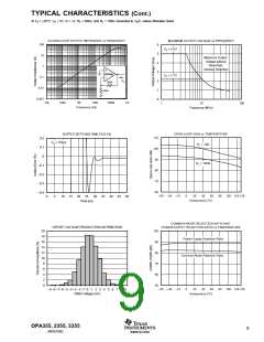
At TA = +25°C, RF = 604Ω, RL = 150Ω, and connected to VS/2, unless otherwise noted.
OPA355
OPA2355
OPA3355
PARAMETER
CONDITION
MIN
TYP
MAX
UNITS
OFFSET VOLTAGE
Input Offset Voltage
VOS
VS = +5V
±2
±9
mV
mV
Specified Temperature Range
Specified Temperature Range
VS = +2.7V to +5.5V, VCM = VS/2 – 0.15V
±15
vs Temperature
dVOS/dT
±7
±80
µV/°C
µV/V
vs Power Supply
PSRR
±350
INPUT BIAS CURRENT
Input Bias Current
IB
3
±50
±50
pA
pA
Input Offset Current
IOS
±1
NOISE
√Hz
nV/
Input Noise Voltage Density
Current Noise Density
en
in
f = 1MHz
f = 1MHz
5.8
50
√Hz
fA/
INPUT VOLTAGE RANGE
Common-Mode Voltage Range
Common-Mode Rejection Ratio
VCM
(V–) – 0.1
(V+) – 1.5
V
CMRR
VS = +5.5V, –0.1V < VCM < +4.0V
66
80
dB
Specified Temperature Range
66
dB
INPUT IMPEDANCE
Differential
1013 || 1.5
1013 || 1.5
Ω || pF
Ω || pF
Common-Mode
OPEN-LOOP GAIN
VS = +5V, 0.3V < VO < 4.7V
VS = +5V, 0.3V < VO < 4.7V
VS = +5V, 0.4V < VO < 4.6V
84
80
80
92
dB
dB
dB
OPA355
OPA2355, OPA3355
FREQUENCY RESPONSE
Small-Signal Bandwidth
f–3dB
f–3dB
f–3dB
f–3dB
GBW
f0.1dB
SR
G
= +1, VO = 100mVp-p, RF = 0Ω
= +2, VO = 100mVp-p, RL = 50Ω
= +2, VO = 100mVp-p, RL = 150Ω
= +2, VO = 100mVp-p, RL = 1kΩ
G = +10, RL = 1kΩ
450
100
170
200
200
75
MHz
MHz
MHz
MHz
MHz
MHz
V/µs
ns
G
G
G
Gain-Bandwidth Product
Bandwidth for 0.1dB Gain Flatness
Slew Rate
G
= +2, VO = 100mVp-p, RF = 560Ω
VS = +5V, G = +2, 4V Output Step
G = +2, VO = 200mVp-p, 10% to 90%
300/–360
2.4
Rise-and-Fall Time
G
= +2, VO = 2Vp-p, 10% to 90%
8
ns
Settling Time, 0.1%
0.01%
VS = +5V, G = +2, 2V Output Step
VS = +5V, G = +2, 2V Output Step
VIN • Gain = VS
30
ns
120
8
ns
Overload Recovery Time
Harmonic Distortion
2nd-Harmonic
ns
G = +2, f = 1MHz, VO = 2Vp-p, RL = 200Ω
G = +2, f = 1MHz, VO = 2Vp-p, RL = 200Ω
NTSC, RL = 150Ω
–81
–93
0.02
0.05
–90
–70
dBc
dBc
%
3rd-Harmonic
Differential Gain Error
Differential Phase Error
Channel-to-Channel Crosstalk
NTSC, RL = 150Ω
degrees
dB
OPA2355
OPA3355
f = 5MHz
f = 5MHz
dB
OUTPUT
Voltage Output Swing from Rail
Voltage Output Swing from Rail
Output Current, Continuous(1)
Output Current, Peak(1)
V
S = +5V, RL = 150Ω, AOL > 84dB
0.2
0.1
0.3
V
V
V
S = +5V, RL = 1kΩ
IO
IO
IO
±60
±100
±80
0.02
mA
mA
mA
Ω
VS = +5V
VS = +3V
f < 100kHz
Output Current, Peak(1)
Closed-Loop Output Impedance
POWER SUPPLY
Specified Voltage Range
Operating Voltage Range
Quiescent Current (per amplifier)
VS
IQ
2.7
5.5
V
V
2.5 to 5.5
8.3
VS = +5V, Enabled, IO = 0
Specified Temperature Range
11
mA
mA
14
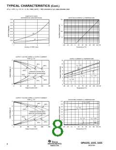
NOTES: (1) See typical characteristic Output Voltage Swing vs Output Current. (2) Logic LOW and HIGH levels are CMOS logic compatible. They are referenced to V–.
OPA355, 2355, 3355
3
SBOS195D
www.ti.com

 TI [ TEXAS INSTRUMENTS ]