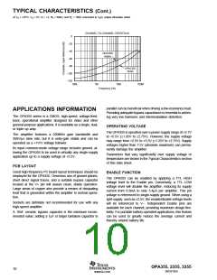
The Enable input can be modeled as a CMOS input gate with
a 100kΩ pull-up resistor to V+. Left open, the Enable pin will
assume a logic HIGH, and the amplifier will be on.
driver. A properly back-terminated 75Ω cable does not ap-
pear as capacitance; it presents only a 150Ω resistive load to
the OPA355 output.
The Enable time is 100ns and the disable time is only 30ns.
This allows the OPA355 to be operated as a “gated” amplifier,
or to have its output multiplexed onto a common output bus.
When disabled, the output assumes a high-impedance state.
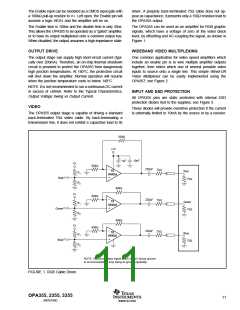
The OPA355 can be used as an amplifier for RGB graphic
signals, which have a voltage of zero at the video black
level, by offsetting and AC-coupling the signal, as shown in
Figure 1.
OUTPUT DRIVE
WIDEBAND VIDEO MULTIPLEXING
The output stage can supply high short-circuit current (typi-
cally over 200mA). Therefore, an on-chip thermal shutdown
circuit is provided to protect the OPA355 from dangerously
high junction temperatures. At 160°C, the protection circuit
will shut down the amplifier. Normal operation will resume
when the junction temperature cools to below 140°C.
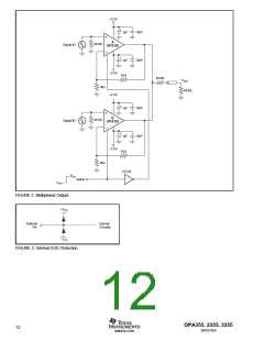
One common application for video speed amplifiers which
include an enable pin is to wire multiple amplifier outputs
together, then select which one of several possible video
inputs to source onto a single line. This simple Wired-OR
Video Multiplexer can be easily implemented using the
OPA357; see Figure 2.
NOTE: it is not recommended to run a continuous DC current
in excess of ±60mA. Refer to the Typical Characteristics,
Output Voltage Swing vs Output Current.
INPUT AND ESD PROTECTION
All OPA355 pins are static protected with internal ESD
protection diodes tied to the supplies; see Figure 3.
VIDEO
These diodes will provide overdrive protection if the current
is externally limited to 10mA by the source or by a resistor.
The OPA355 output stage is capable of driving a standard
back-terminated 75Ω video cable. By back-terminating a
transmission line, it does not exhibit a capacitive load to its
604Ω
+3V
+
1µF
10nF
V+
604Ω
220µF
75Ω
1/3
OPA355
Red
75Ω
R1
R2
Red(1)
604Ω
V+
604Ω
220µF
75Ω
1/3
OPA355
Green
R1
R2
Green(1)
75Ω
604Ω
V+
604Ω
220µF
75Ω
1/3
OPA355
Blue
R1
R2
Blue(1)
75Ω
NOTE: (1) Source video signal offset 300mV above ground
to accommodate op amp swing-to-ground capability.
FIGURE 1. RGB Cable Driver.
OPA355, 2355, 3355
11
SBOS195D
www.ti.com

 TI [ TEXAS INSTRUMENTS ]