TYPICAL CHARACTERISTICS (Cont.)
At TA = +25°C, VS = 5V, G = +2, RF = 604Ω, and RL = 150Ω connected to VS/2, unless otherwise noted.
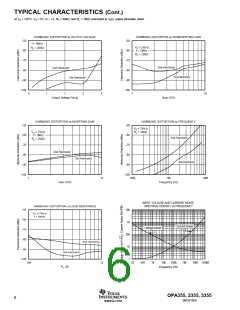
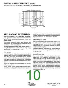
CHANNEL-TO-CHANNEL CROSSTALK
0
–20
–40
OPA3355
(triple)
–60
–80
OPA2355
(dual)
–100
–120
100k
1M
10M
100M
Frequency (Hz)
parallel can be beneficial when driving a low-resistance load.
Providing adequate bypass capacitance is essential to achiev-
ing very low harmonic and intermodulation distortion.
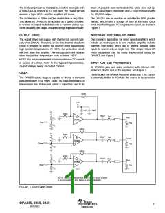
APPLICATIONS INFORMATION
The OPA355 series is a CMOS, high-speed, voltage-feed-
back, operational amplifier designed for video and other
general-purpose applications. It is available as a single, dual,
or triple op amp.
OPERATING VOLTAGE
The OPA355 is specified over a power-supply range of +2.7V
to +5.5V (±1.35V to ±2.75V). However, the supply voltage
may range from +2.5V to +5.5V (±1.25V to ±2.75V). Supply
voltages higher than 7.5V (absolute maximum) can perma-
nently damage the amplifier.
The amplifier features a 200MHz gain bandwidth and
360V/µs slew rate, but it is unity-gain stable and can be
operated as a +1V/V voltage follower.
Its input common-mode voltage range includes ground, al-
lowing the OPA355 to be used in virtually any single-supply
application up to a supply voltage of +5.5V.
Parameters that vary significantly over supply voltage or
temperature are shown in the Typical Characteristics section
of this data sheet.
PCB LAYOUT
Good high-frequency PC board layout techniques should be
employed for the OPA355. Generous use of ground planes,
short direct signal traces, and a suitable bypass capacitor
located at the V+ pin will assure clean, stable operation.
Large areas of copper also provide a means of dissipating
heat that is generated within the amplifier in normal opera-
tion.
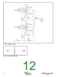
ENABLE FUNCTION
The OPA355 can be enabled by applying a TTL HIGH
voltage level to the Enable pin. Conversely, a TTL LOW
voltage level will disable the amplifier, reducing its supply
current from 8.3mA to only 3.4µA per amplifier. This pin
voltage is referenced to single-supply ground. When using a
split-supply, such as ±2.5V, the enable/disable voltage levels
will be referenced to V–. Independent Enable pins are
available for each channel, providing maximum design flex-
ibility. For portable battery-operated applications, this feature
can be used to greatly reduce the average current and
thereby extend battery life.
Sockets are definitely not recommended for use with any
high-speed amplifier.
A 10nF ceramic bypass capacitor is the minimum recom-
mended value; adding a 1µF or larger tantalum capacitor in
OPA355, 2355, 3355
10
SBOS195D
www.ti.com

 TI [ TEXAS INSTRUMENTS ]