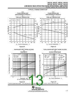
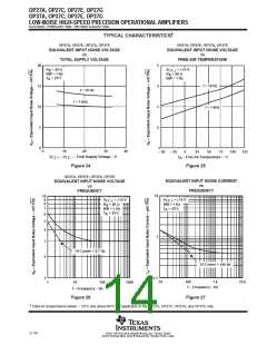
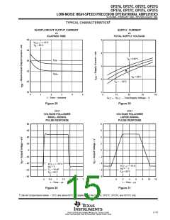
OP27A, OP27C, OP27E, OP27G
OP37A, OP37C, OP37E, OP37G
LOW-NOISE HIGH-SPEED PRECISION OPERATIONAL AMPLIFIERS
SLOS100B – FEBRUARY 1989 – REVISED AUGUST 1994
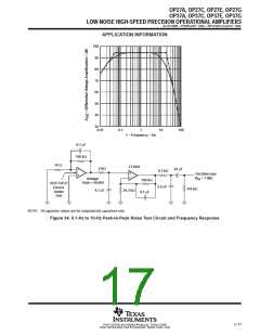
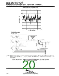
APPLICATION INFORMATION
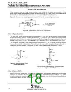
offset voltage and drift (continued)
The circuit shown in Figure 38 measures offset voltage. This circuit can also be used as the burn-in configuration
for the OP27 and OP37 with the supply voltage increased to 20 V, R1 = R3 = 10 kΩ, R2 = 200 Ω, and
A
= 100.
VD
R1
50 kΩ
15 V
7
2
3
–
+
6
R2
100 Ω
V
O
= 1000 V
IO
4
R3
50 kΩ
–15 V
NOTE A: Resistors must have low thermoelectric potential.
Figure 38. Test Circuit for Offset Voltage and Offset Voltage
Temperature Coefficient
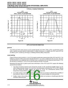
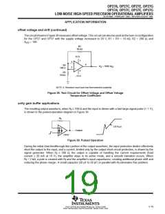
unity gain buffer applications
The resulting output waveform, when R ≤ 100 Ω and the input is driven with a fast large-signal pulse (> 1 V),
f
is shown in the pulsed-operation diagram in Figure 39.
R
f
2.8 V/µs
–
Output
+
OP27
Figure 39. Pulsed Operation
During the initial (fast-feedthrough-like) portion of the output waveform, the input protection diodes effectively
short the output to the input, and a current, limited only by the output short-circuit protection, is drawn by the
signal generator. When R ≥ 500 Ω, the output is capable of handling the current requirements (load
f
current ≤ 20 mA at 10 V), the amplifier stays in its active mode, and a smooth transition occurs. When
R > 2 kΩ, a pole is created with R and the amplifier’s input capacitance, creating additional phase shift and
f
f
reducing the phase margin. A small capacitor (20 pF to 50 pF) in parallel with R eliminates this problem.
f
2–19
POST OFFICE BOX 655303 • DALLAS, TEXAS 75265
POST OFFICE BOX 1443 • HOUSTON, TEXAS 77251–1443

 TI [ TEXAS INSTRUMENTS ]