OP27A, OP27C, OP27E, OP27G
OP37A, OP37C, OP37E, OP37G
LOW-NOISE HIGH-SPEED PRECISION OPERATIONAL AMPLIFIERS
SLOS100B – FEBRUARY 1989 – REVISED AUGUST 1994
APPLICATION INFORMATION
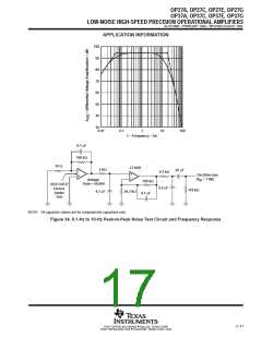
When measuring noise on a large number of units, a noise-voltage density test is recommended. A 10-Hz
noise-voltage density measurement correlates well with a 0.1-Hz to 10-Hz peak-to-peak noise reading since
both results are determined by the white noise and the location of the 1/f corner frequency.
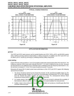
Figure 35 shows a circuit measuring current noise and the formula for calculating current noise.
10kΩ
100 Ω
500 kΩ
500 kΩ
2
2 1/2
– (130 nV) ]
–
+
[V
no
V
no
I =
n
1 MΩ × 100
Figure 35. Current Noise Test Circuit and Formula
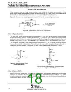
offset voltage adjustment
The input offset voltage and temperature coefficient of the OP27 and OP37 are permanently trimmed to a low
level at wafer testing. However, if further adjustment of V is necessary, using a 10-kΩ nulling potentiometer
IO
as shown in Figure 36 does not degrade the temperature coefficient α
. Trimming to a value other than zero
VIO
creates an α
of V /300 µV/°C. For example, if V is adjusted to 300 µV, the change in α
is 1 µV/°C.
VIO
IO
IO
VIO
The adjustment range with a 10-kΩ potentiometer is approximately ±2.5 mV. If a smaller adjustment range is
needed, the sensitivity and resolution of the nulling can be improved by using a smaller potentiometer in
conjunction with fixed resistors. The example in Figure 37 has an approximate null range of ±200 µV.
4.7 kΩ
10 kΩ
1 kΩ
15 V
15 V
1
2
3
8
4.7 kΩ
–
+
7
6
Input
Output
1
2
3
8
4
4
7
6
Input
Output
–15 V
Figure 36. Standard Input Offset
Voltage Adjustment
–15 V
Figure 37. Input Offset Voltage Adjustment With
Improved Sensitivity
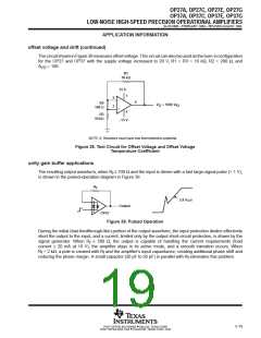
offset voltage and drift
Unless proper care is exercised, thermoelectric effects caused by temperature gradients across dissimilar
metals at the contacts to the input terminals can exceed the inherent temperature coefficient of the
V
IO
amplifier. Air currents should be minimized, package leads should be short, and the two input leads should be
close together and at the same temperature.
2–18
POST OFFICE BOX 655303 • DALLAS, TEXAS 75265
POST OFFICE BOX 1443 • HOUSTON, TEXAS 77251–1443

 TI [ TEXAS INSTRUMENTS ]