MC33063A
MC34063A
SLLS636L –DECEMBER 2004–REVISED DECEMBER 2009
www.ti.com
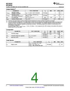
Output Switch(1)
PARAMETER
TEST CONDITIONS
ISW = 1 A, pins 1 and 8 connected
TA
MIN
TYP
MAX UNIT
Saturation voltage –
VCE(sat)
VCE(sat)
Full range
1
1.3
0.7
V
V
Darlington connection
Saturation voltage –
ISW = 1 A, RPIN8 = 82 Ω to VCC
,
Full range
0.45
non-Darlington connection(2)
forced β ~ 20
hFE
DC current gain
ISW = 1 A, VCE = 5 V
VCE = 40 V
25°C
50
75
IC(off)
Collector off-state current
Full range
0.01
100
μA
(1) Low duty-cycle pulse testing is used to maintain junction temperature as close to ambient temperature as possible.
(2) In the non-Darlington configuration, if the output switch is driven into hard saturation at low switch currents (≤300 mA) and high driver
currents (≥30 mA), it may take up to 2 μs for the switch to come out of saturation. This condition effectively shortens the off time at
frequencies ≥30 kHz, becoming magnified as temperature increases. The following output drive condition is recommended in the
non-Darlington configuration:
Forced β of output switch = IC,SW / (IC,driver – 7 mA) ≥ 10, where ~7 mA is required by the 100-Ω resistor in the emitter of the driver to
forward bias the Vbe of the switch.
Comparator
PARAMETER
TEST CONDITIONS
TA
MIN
1.225
1.21
TYP
MAX UNIT
25°C
1.25
1.275
V
Vth
Threshold voltage
Full range
Full range
Full range
1.29
ΔVth
Threshold-voltage line regulation
Input bias current
VCC = 5 V to 40 V
VIN = 0 V
1.4
5
mV
nA
IIB
–20
–400
Total Device
PARAMETER
TEST CONDITIONS
TA
Full range
MIN
MAX UNIT
mA
VCC = 5 V to 40 V, CT = 1 nF,
VPIN7 = VCC, VPIN5 > Vth,
ICC
Supply current
4
VPIN2 = GND, All other pins open
4
Submit Documentation Feedback
Copyright © 2004–2009, Texas Instruments Incorporated
Product Folder Link(s): MC33063A MC34063A

 TI [ TEXAS INSTRUMENTS ]