MC33063A
MC34063A
www.ti.com
SLLS636L –DECEMBER 2004–REVISED DECEMBER 2009
1.5-A PEAK BOOST/BUCK/INVERTING SWITCHING REGULATORS
Check for Samples: MC33063A MC34063A
1
FEATURES
•
•
•
•
Wide Input Voltage Range: 3 V to 40 V
•
•
•
Precision Internal Reference: 2%
High Output Switch Current: Up to 1.5 A
Adjustable Output Voltage
Short-Circuit Current Limiting
Low Standby Current
Oscillator Frequency Up to 100 kHz
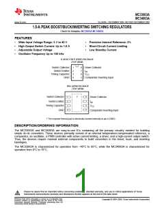
D (SOIC) OR P (PDIP) PACKAGE
(TOP VIEW)
Switch Collector
Switch Emitter
Timing Capacitor
GND
1
2
3
4
8
7
6
5
Driver Collector
Ipk
VCC
Comparator Inverting Input
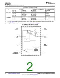
DRJ (QFN) PACKAGE
(TOP VIEW)
†
Switch Collector
8
1
Driver Collector
2
3
4
Switch Emitter
7
6
5
Ipk
Timing Capacitor
VCC
GND
Comparator Inverting Input
†
The exposed thermal pad is electrically bonded internally to pin 4 (GND) .
DESCRIPTION/ORDERING INFORMATION
The MC33063A and MC34063A are easy-to-use ICs containing all the primary circuitry needed for building
simple dc-dc converters. These devices primarily consist of an internal temperature-compensated reference, a
comparator, an oscillator, a PWM controller with active current limiting, a driver, and a high-current output switch.
Thus, the devices require minimal external components to build converters in the boost, buck, and inverting
topologies.
The MC33063A is characterized for operation from –40°C to 85°C, while the MC34063A is characterized for
operation from 0°C to 70°C.
1
Please be aware that an important notice concerning availability, standard warranty, and use in critical applications of Texas
Instruments semiconductor products and disclaimers thereto appears at the end of this data sheet.
PRODUCTION DATA information is current as of publication date.
Copyright © 2004–2009, Texas Instruments Incorporated
Products conform to specifications per the terms of the Texas
Instruments standard warranty. Production processing does not
necessarily include testing of all parameters.

 TI [ TEXAS INSTRUMENTS ]