ꢀ
ꢁ
ꢂ
ꢃ
ꢄ
ꢅ
ꢆ
ꢇ
ꢈ
ꢉ
ꢊ
ꢋ
ꢊ
ꢌ
ꢅ
ꢍ
ꢎ
ꢆ
ꢏ
ꢐ
ꢍ
ꢑ
ꢒ
ꢐ
ꢓ
ꢄ
ꢔ
ꢖ ꢗꢆ ꢘ ꢊ ꢌꢀꢆꢍꢆ ꢔ ꢙ ꢐꢆ ꢓꢐ ꢆꢀ
ꢎ
ꢐ
ꢀ
ꢎ
ꢐ
ꢕ
ꢕ
ꢔ
ꢒ
SCBS133F − MAY 1992 − REVISED OCTOBER 2003
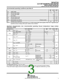
recommended operating conditions (see Note 4)
MIN
2.7
2
MAX
UNIT
V
V
V
V
V
Supply voltage
3.6
CC
High-level input voltage
Low-level input voltage
Input voltage
V
IH
0.8
5.5
−32
64
V
IL
V
I
I
I
High-level output current
Low-level output current
Input transition rise or fall rate
Operating free-air temperature
mA
mA
ns/V
°C
OH
OL
∆t/∆v
Outputs enabled
10
T
A
−40
85
NOTE 4: All unused inputs of the device must be held at V
or GND to ensure proper device operation. Refer to the TI application report,
CC
Implications of Slow or Floating CMOS Inputs, literature number SCBA004.
electrical characteristics over recommended operating free-air temperature range (unless
otherwise noted)
†
TYP
PARAMETER
TEST CONDITIONS
I = −18 mA
MIN
MAX
UNIT
V
IK
V
V
V
V
= 2.7 V,
−1.2
V
CC
CC
CC
CC
I
‡
= MIN to MAX ,
= 2.7 V,
I
I
I
I
I
I
I
I
= −100 µA
= −8 mA
= −32 mA
= 100 µA
= 24 mA
= 16 mA
= 32 mA
= 64 mA
V
−0.2
OH
OH
OH
OL
OL
OL
OL
OL
CC
2.4
2
V
V
V
OH
= 3 V
0.2
0.5
0.4
0.5
0.55
10
V
CC
= 2.7 V
V
OL
V
V
= 3 V
CC
‡
= 0 or MAX ,
V = 5.5 V
I
CC
V = V
I
or GND
Control inputs
Data inputs
1
CC
CC
I
I
µA
V = V
I
1
V
CC
= 3.6 V
V = 0
I
−5
I
I
V
V
= 0,
V or V = 0 to 4.5 V
100
µA
µA
off
CC
I
O
V = 0.8 V
I
75
= 3 V
Data inputs
I(hold)
CC
V = 2 V
I
−75
I
I
V
V
= 3.6 V,
= 3.6 V,
V
= 3 V
5
−5
µA
µA
OZH
CC
O
O
V
= 0.5 V
OZL
CC
Outputs high
Outputs low
0.12
4.5
0.19
7
V
= 3.6 V,
I
O
= 0,
CC
I
mA
CC
V = V
I
or GND
CC
Outputs disabled
0.12
0.19
V
CC
= 3 V to 3.6 V,
One input at V
CC
− 0.6 V, Other inputs at V
or GND
CC
§
0.2
mA
∆I
CC
C
C
V = 3 V or 0
4
8
pF
pF
i
I
V
O
= 3 V or 0
o
†
‡
§
All typical values are at V
CC
= 3.3 V, T = 25°C.
A
For conditions shown as MIN or MAX, use the appropriate value specified under recommended operating conditions.
This is the increase in supply current for each input that is at the specified TTL voltage level, rather than V
or GND.
CC
3
POST OFFICE BOX 655303 • DALLAS, TEXAS 75265

 TI [ TEXAS INSTRUMENTS ]