SN74LVC245A
OCTAL BUS TRANSCEIVER
WITH 3-STATE OUTPUTS
www.ti.com
SCAS218T–JANUARY 1993–REVISED FEBRUARY 2005
DESCRIPTION/ORDERING INFORMATION (CONTINUED)
To ensure the high-impedance state during power up or power down, OE should be tied to VCC through a pullup
resistor; the minimum value of the resistor is determined by the current-sinking capability of the driver.
Inputs can be driven from either 3.3-V or 5-V devices. This feature allows the use of this device as a translator in
a mixed 3.3-V/5-V system environment.
This device is fully specified for partial-power-down applications using Ioff. The Ioff circuitry disables the outputs,
preventing damaging current backflow through the device when it is powered down.
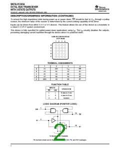
GQN OR ZQN PACKAGE
(TOP VIEW)
1
2
3
4
A
B
C
D
E
TERMINAL ASSIGNMENTS
1
A1
2
3
4
A
B
C
D
E
DIR
B2
A4
B6
A8
VCC
A2
B4
A6
B8
OE
B1
B3
B5
B7
A3
A5
A7
GND
FUNCTION TABLE
INPUTS
OPERATION
OE
L
DIR
L
B data to A bus
A data to B bus
Isolation
L
H
H
X
LOGIC DIAGRAM (POSITIVE LOGIC)
1
2
DIR
A1
19
OE
B1
18
To Seven Other Channels
Pin numbers shown are for the DB, DGV, DW, N, NS, PW, and RGY packages.
2

 TI [ TEXAS INSTRUMENTS ]