SN74LVC244A
OCTAL BUFFER/DRIVER
WITH 3-STATE OUTPUTS
www.ti.com
SCAS414X–NOVEMBER 1992–REVISED MARCH 2005
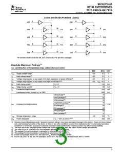
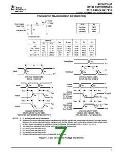
LOGIC DIAGRAM (POSITIVE LOGIC)
1
2
19
1OE
1A1
2OE
18
16
14
12
11
9
7
5
3
1Y1
1Y2
1Y3
1Y4
2A1
2Y1
2Y2
2Y3
2Y4
4
6
8
13
15
17
1A2
1A3
1A4
2A2
2A3
2A4
Pin numbers shown are for the DB, DGV, DW, N, NS, PW, and RGY packages.
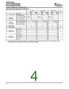
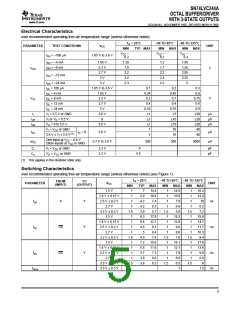
Absolute Maximum Ratings(1)
over operating free-air temperature range (unless otherwise noted)
MIN
–0.5
–0.5
–0.5
MAX UNIT
VCC Supply voltage range
6.5
6.5
6.5
V
V
VI
Input voltage range(2)
VO
VO
IIK
Voltage range applied to any output in the high-impedance or power-off state(2)
Voltage range applied to any output in the high or low state(2)(3)
V
–0.5 VCC + 0.5
V
Input clamp current
VI < 0
–50
–50
±50
±100
70
mA
mA
mA
mA
IOK
IO
Output clamp current
VO < 0
Continuous output current
Continuous current through VCC or GND
DB package(4)
DGV package(4)
DW package(4)
GQN/ZQN package(4)
N package(4)
92
58
78
θJA
Package thermal impedance
°C/W
69
NS package(4)
PW package(4)
RGY package(5)
60
83
37
Tstg
Ptot
Storage temperature range
Power dissipation
–65
150
500
°C
TA = –40°C to 125°C(6)(7)
mW
(1) Stresses beyond those listed under "absolute maximum ratings" may cause permanent damage to the device. These are stress ratings
only, and functional operation of the device at these or any other conditions beyond those indicated under "recommended operating
conditions" is not implied. Exposure to absolute-maximum-rated conditions for extended periods may affect device reliability.
(2) The input and output negative-voltage ratings may be exceeded if the input and output current ratings are observed.
(3) The value of VCC is provided in the recommended operating conditions table.
(4) The package thermal impedance is calculated in accordance with JESD 51-7.
(5) The package thermal impedance is calculated in accordance with JESD 51-5.
(6) For the DW package: above 70°C the value of Ptot derates linearly with 8 mW/K.
(7) For the DB, DGV, N, NS, and PW packages: above 60°C the value of Ptot derates linearly with 5.5 mW/K.
3

 TI [ TEXAS INSTRUMENTS ]