SN74LVC244A
OCTAL BUFFER/DRIVER
WITH 3-STATE OUTPUTS
www.ti.com
SCAS414X–NOVEMBER 1992–REVISED MARCH 2005
DESCRIPTION/ORDERING INFORMATION (CONTINUED)
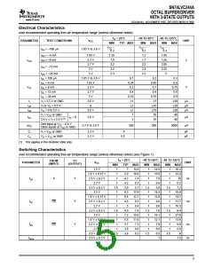
The SN74LVC244A is organized as two 4-bit line drivers with separate output-enable (OE) inputs. When OE is
low, the device passes data from the A inputs to the Y outputs. When OE is high, the outputs are in the
high-impedance state.
Inputs can be driven from either 3.3-V or 5-V devices. This feature allows the use of this device as a translator in
a mixed 3.3-V/5-V system environment.
To ensure the high-impedance state during power up or power down, OE should be tied to VCC through a pullup
resistor; the minimum value of the resistor is determined by the current-sinking capability of the driver.
This device is fully specified for partial-power-down applications using Ioff. The Ioff circuitry disables the outputs,
preventing damaging current backflow through the device when it is powered down.
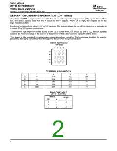
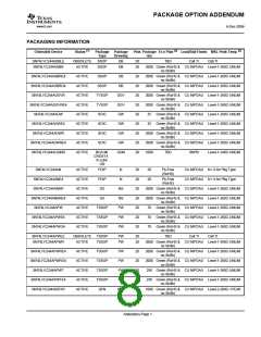
GQN OR ZQN PACKAGE
(TOP VIEW)
1
2
3
4
A
B
C
D
E
TERMINAL ASSIGNMENTS
1
2
3
4
A
B
C
D
E
1A1
1A2
1A3
1A4
GND
1OE
2A4
2Y3
2A2
2Y1
VCC
2Y4
2A3
2Y2
2A1
2OE
1Y1
1Y2
1Y3
1Y4
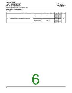
FUNCTION TABLE
(EACH BUFFER)
INPUTS
OUTPUT
Y
OE
L
A
H
L
H
L
L
H
X
Z
2

 TI [ TEXAS INSTRUMENTS ]