LT1007, LT1007A, LT1037, LT1037A
LOW-NOISE, HIGH-SPEED, PRECISION OPERATIONAL AMPLIFIERS
SLOS017C – D3195, FEBRUARY 1989 – REVISED JANUARY 1993
APPLICATION INFORMATION
1 kΩ
V
CC+
10 kΩ
4.7 kΩ
V
CC+
4.7 kΩ
–
–
IN–
IN+
IN–
IN+
OUT
OUT
+
+
4
V
CC–
V
CC–
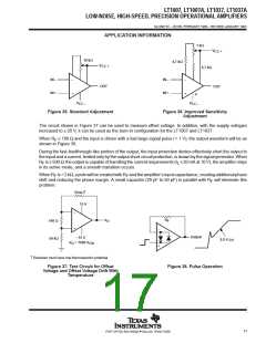
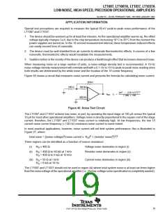
Figure 35. Standard Adjustment
Figure 36. Improved Sensitivity
Adjustment
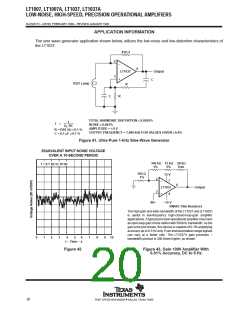
The circuit shown in Figure 37 can be used to measure offset voltage. In addition, with the supply voltages
increased to ± 20 V, it can be used as the burn-in configuration for the LT1007 and LT1037.
When R ≤ 100 Ω and the input is driven with a fast large-signal pulse (> 1 V), the output waveform will be as
F
shown in Figure 38.
During the fast-feedthrough-like portion of the output, the input protection diodes effectively short the output to
the input and a current, limited only by the output short-circuit protection, is drawn by the signal generator. When
R is ≥ 500 Ω, the output is capable of handling the current requirements (I ≤ 20 mA at 10 V), the amplifier stays
F
L
in its active mode, and a smooth transition occurs.
When R is > 2 kΩ, a pole will be created with R and the amplifier’s input capacitance, creating additional phase
F
F
shift and reducing the phase margin. A small capacitor (20 pF to 50 pF) in parallel with R will eliminate this
F
problem.
†
50 kΩ
15 V
–
+
R
V
O
100 Ω
50 kΩ
F
–
+
Output
–15 V
= 1000 V
2.8 V /µs
V
O
OS
†
Resistors must have low thermoelectric potential
Figure 37. Test Circuit for Offset
Voltage and Offset Voltage Drift With
Temperature
Figure 38. Pulse Operation
17
POST OFFICE BOX 655303 • DALLAS, TEXAS 75265

 TI [ TEXAS INSTRUMENTS ]