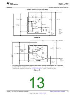
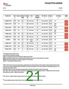
LP2987, LP2988
www.ti.com
SNVS004J –MARCH 1999–REVISED APRIL 2013
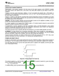
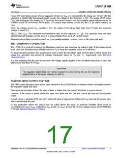
Power-ON reset delay occurs when a capacitor (shown as CDLY) is connected to the Delay pin. At turn-ON, this
capacitor is initially fully discharged (which means the voltage at the Delay pin is 0V). The output of U1 keeps
CDLY fully discharged (by sinking the 2.2 µA from the current source) until the regulator output voltage comes up
to within about 5% of nominal. At this point, U1's output stops sinking current and the 2.2 µA starts charging up
CDLY
.
When the voltage across CDLY reaches 1.23V, the output of U2 will go high (note that D1 limits the maximum
voltage to about 2V).
SELECTING CDLY: The maximum recommended value for this capacitor is 1 µF. The capacitor must not have
excessively high leakage current, since it is being charged from a 2.2 µA current source.
Aluminum electrolytics can not be used, but good-quality tantalum, ceremic, mica, or film types will work.
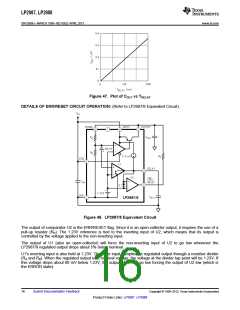
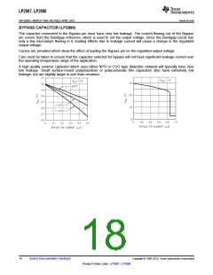
SHUTDOWN INPUT OPERATION
The LP2987/8 is shut off by driving the Shutdown input low, and turned on by pulling it high. If this feature is not
to be used, the Shutdown input should be tied to VIN to keep the regulator output on at all times.
To assure proper operation, the signal source used to drive the Shutdown input must be able to swing above and
below the specified turn-on/turn-off voltage thresholds listed as VH and VL, respectively (see Electrical
Characteristics).
It is also important that the turn-on (and turn-off) voltage signals applied to the Shutdown input have a slew rate
which is not less than 40 mV/µs.
CAUTION
The regulator output state can not be ensured if a slow-moving AC (or DC) signal is
applied that is in the range between VH and VL.
REVERSE INPUT-OUTPUT VOLTAGE
The PNP power transistor used as the pass element in the LP2987/8 has an inherent diode connected between
the regulator output and input.
During normal operation (where the input voltage is higher than the output) this diode is reverse-biased.
However, if the output is pulled above the input, this diode will turn ON and current will flow into the regulator
output.
In such cases, a parasitic SCR can latch which will allow a high current to flow into VIN (and out the ground pin),
which can damage the part.
In any application where the output may be pulled above the input, an external Schottky diode must be
connected from VIN to VOUT (cathode on VIN, anode on VOUT), to limit the reverse voltage across the LP2987/8 to
0.3V (see Absolute Maximum Ratings).
Copyright © 1999–2013, Texas Instruments Incorporated
Submit Documentation Feedback
17
Product Folder Links: LP2987 LP2988

 TI [ TEXAS INSTRUMENTS ]