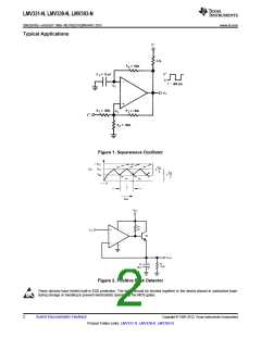
LMV331-N, LMV339-N, LMV393-N
www.ti.com
SNOS018G –AUGUST 1999–REVISED FEBRUARY 2013
(1)(2)
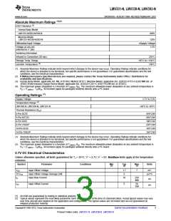
Absolute Maximum Ratings
ESD Tolerance
(3)
Human Body Model
LMV331-N/393-N/339-N
800V
Machine Model
LMV331-N/339-N/393-N
120V
±Supply Voltage
5.5V
Differential Input Voltage
Voltage on any pin
(referred to V− pin)
Soldering Information
Infrared or Convection (20 sec)
235°C
−65°C to +150°C
150°C
Storage Temp. Range
(4)
Junction Temperature
(1) Absolute Maximum Ratings indicate limits beyond which damage to the device may occur. Operating Ratings indicate conditions for
which the device is intended to be functional, but specific performance is not guaranteed. For guaranteed specifications and the test
conditions, see the Electrical characteristics.
(2) If Military/Aerospace specified devices are required, please contact the Texas Instruments Sales Office / Distributors for
availability and specifications.
(3) Human Body Model, applicable std. MIL-STD-883, Method 3015.7. Machine Model, applicable std. JESD22-A115-A (ESD MM std. of
JEDEC)Field-Induced Charge-Device Model, applicable std. JESD22-C101-C (ESD FICDM std. of JEDEC).
(4) The maximum power dissipation is a function of TJ(MAX), θJA. The maximum allowable power dissipation at any ambient temperature is
PD = (TJ(MAX) - TA)/θJA. All numbers apply for packages soldered directly onto a PC board.
(1)
Operating Ratings
Supply Voltage
2.7V to 5.0V
(2)
Temperature Range
LMV393-N. LMV339-N, LMV331-N
−40°C to +85°C
Thermal Resistance (θJA
)
5-Pin SC70
478°C/W
265°C/W
190°C/W
235°C/W
145°C/W
155°C/W
5-Pin SOT23
8-Pin SOIC
8-Pin VSSOP
14-Pin SOIC
14-Pin TSSOP
(1) Absolute Maximum Ratings indicate limits beyond which damage to the device may occur. Operating Ratings indicate conditions for
which the device is intended to be functional, but specific performance is not guaranteed. For guaranteed specifications and the test
conditions, see the Electrical characteristics.
(2) The maximum power dissipation is a function of TJ(MAX), θJA. The maximum allowable power dissipation at any ambient temperature is
PD = (TJ(MAX) - TA)/θJA. All numbers apply for packages soldered directly onto a PC board.
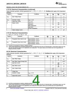
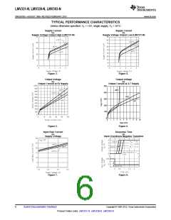
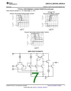
2.7V DC Electrical Characteristics
Unless otherwise specified, all limits guaranteed for TJ = 25°C, V+ = 2.7V, V− = 0V. Boldface limits apply at the temperature
extremes.
Symbol
Parameter
Input Offset Voltage
Conditions
Min
Typ
Max
Units
(1)
(2)
(1)
VOS
1.7
5
7
mV
TCVOS
IB
Input Offset Voltage Average Drift
Input Bias Current
µV/°C
10
250
400
nA
nA
IOS
Input Offset Current
5
50
150
(1) All limits are guaranteed by testing or statistical analysis.
(2) Typical values represent the most likely parametric norm as determined at the time of characterization. Actual typical values may vary
over time and will also depend on the application and configuration. The typical values are not tested and are not guaranteed on
shipped production material.
Copyright © 1999–2013, Texas Instruments Incorporated
Submit Documentation Feedback
3
Product Folder Links: LMV331-N LMV339-N LMV393-N

 TI [ TEXAS INSTRUMENTS ]