LMT86, LMT86-Q1
www.ti.com
SNIS169A –MARCH 2013–REVISED JUNE 2013
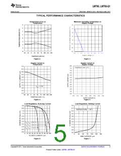
OUTPUT AND NOISE CONSIDERATIONS
A push-pull output gives the LMT86/LMT86-Q1 the ability to sink and source significant current. This is beneficial
when, for example, driving dynamic loads like an input stage on an analog-to-digital converter (ADC). In these
applications the source current is required to quickly charge the input capacitor of the ADC. See the
APPLICATION CIRCUITS section for more discussion of this topic. The LMT86/LMT86-Q1 is ideal for this and
other applications which require strong source or sink current.
The LMT86/LMT86-Q1's supply-noise gain (the ratio of the AC signal on VOUT to the AC signal on VDD) was
measured during bench tests. Its typical attenuation is shown in the TYPICAL PERFORMANCE
CHARACTERISTICS section. A load capacitor on the output can help to filter noise.
For operation in very noisy environments, some bypass capacitance should be present on the supply within
approximately 5 centimeters of the LMT86/LMT86-Q1.
CAPACITIVE LOADS
The LMT86/LMT86-Q1 handles capacitive loading well. In an extremely noisy environment, or when driving a
switched sampling input on an ADC, it may be necessary to add some filtering to minimize noise coupling.
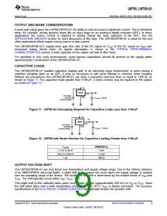
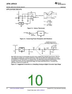
Without any precautions, the LMT86/LMT86-Q1 can drive a capacitive load less than or equal to 1100 pF as
shown in Figure 11. For capacitive loads greater than 1100 pF, a series resistor may be required on the output,
as shown in Figure 12.
V
DD
LMT86
GND
OUT
OPTIONAL
BYPASS
C
LOAD
≤ 1100 pF
CAPACITANCE
Figure 11. LMT86 No Decoupling Required for Capacitive Loads Less than 1100 pF
V
DD
R
S
LMT86
OUT
OPTIONAL
BYPASS
CAPACITANCE
GND
C
LOAD
> 1100 pF
Figure 12. LMT86 with Series Resistor for Capacitive Loading Greater than 1100 pF
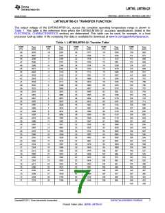
CLOAD
1.1 nF to 99 nF
100 nF to 999 nF
1 μF
MINIMUM RS
3 kΩ
1.5 kΩ
800 Ω
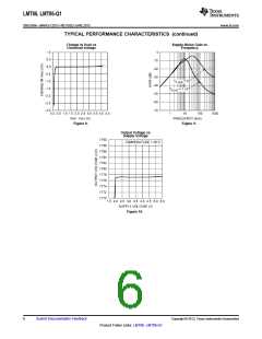
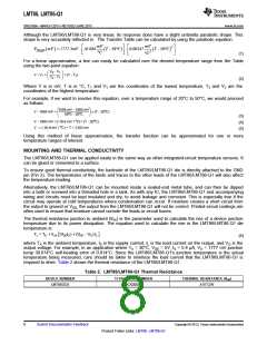
OUTPUT VOLTAGE SHIFT
The LMT86/LMT86-Q1 are very linear over temperature and supply voltage range. Due to the intrinsic behavior
of an NMOS/PMOS rail-to-rail buffer, a slight shift in the output can occur when the supply voltage is ramped
over the operating range of the device. The location of the shift is determined by the relative levels of VDD and
VOUT. The shift typically occurs when VDD- VOUT = 1 V.
This slight shift (a few millivolts) takes place over a wide change (approximately 200 mV) in VDD or VOUT. Since
the shift takes place over a wide temperature change of 5°C to 20°C, VOUT is always monotonic. The accuracy
specifications in the ELECTRICAL CHARACTERISTICS table already include this possible shift.
Copyright © 2013, Texas Instruments Incorporated
Submit Documentation Feedback
9
Product Folder Links: LMT86 LMT86-Q1

 TI [ TEXAS INSTRUMENTS ]