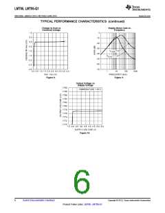
LMT86, LMT86-Q1
SNIS169A –MARCH 2013–REVISED JUNE 2013
www.ti.com
APPLICATION CIRCUITS
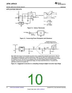
V
TEMP
V+
R3
V
V
T1
R4
T2
R1
V
T
(High = overtemp alarm)
4.1V
U3
+
V
OUT
V
OUT
U1
LM4040
0.1 mF
-
R2
(4.1)R2
V
V
=
=
T1
R1 + R2||R3
LMT86
U2
V
DD
V
Temp
(4.1)R2
T2
R2 + R1||R3
Figure 13. Celsius Thermostat
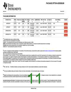
V
V
OUT
DD
SHUTDOWN
LMT86
Any logic
device output
Figure 14. Conserving Power Dissipation with Shutdown
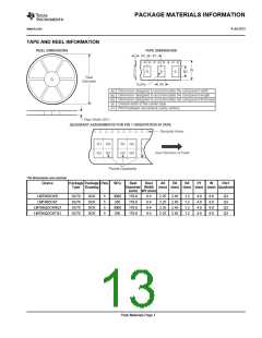
Simplified Input Circuit of
SAR Analog-to-Digital Converter
Reset
+2.7V to +5.5V
Input
Pin
Sample
R
SS
R
MUX
LMT86
V
OUT
DD
GND
C
BP
C
MUX
C
FILTER
C
SAMPLE
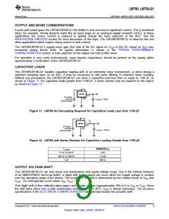
Most CMOS ADCs found in microcontrollers and ASICs have a sampled data comparator input structure. When the
ADC charges the sampling cap, it requires instantaneous charge from the output of the analog source such as the
LMT86/LMT86-Q1 temperature sensor and many op amps. This requirement is easily accommodated by the addition
of a capacitor (CFILTER). The size of CFILTER depends on the size of the sampling capacitor and the sampling
frequency. Since not all ADCs have identical input stages, the charge requirements will vary. This general ADC
application is shown as an example only.
Figure 15. Suggested Connection to a Sampling Analog-to-Digital Converter Input Stage
10
Submit Documentation Feedback
Copyright © 2013, Texas Instruments Incorporated
Product Folder Links: LMT86 LMT86-Q1

 TI [ TEXAS INSTRUMENTS ]