LMT86, LMT86-Q1
SNIS169A –MARCH 2013–REVISED JUNE 2013
www.ti.com
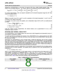
OPERATING RATINGS
VALUE
MIN ≤ TA ≤ TMAX
−50 ≤ TA ≤ 150
2.2 to 5.5
UNIT
°C
T
Specified Temperature Range:
°C
Supply Voltage Range (VDD
Thermal Resistance (θJA
(1)(2) (SOT)
(1) The junction to ambient thermal resistance (θJA) is specified without a heat sink in still air.
)
V
)
415
°C/W
(2) Changes in output due to self heating can be computed by multiplying the internal dissipation by the thermal resistance.
ACCURACY CHARACTERISTICS
These limits do not include DC load regulation. These stated accuracy limits are with reference to the values in Table 1.
(1)
PARAMETER
CONDITIONS
40°C to 150°C; VDD = 2.4 V to 5.5 V
TYPICAL
0.4
LIMITS
2.7
UNIT
°C
0°C to 40°C; VDD = 2.4 V to 5.5 V
0°C to 70°C; VDD = 3.0 V to 5.5 V
–50°C to 0°C; VDD = 3.0 V to 5.5 V
–50°C to 0°C; VDD = 3.6 V to 5.5 V
0.7
2.7
°C
(2)
Temperature Error
0.3
2.7
°C
0.7
2.7
0.25
°C
(1) Limits are specified to TI's AOQL (Average Outgoing Quality Level).
(2) Accuracy is defined as the error between the measured and reference output voltages, tabulated in the Transfer Table at the specified
conditions of supply gain setting, voltage, and temperature (expressed in °C). Accuracy limits include line regulation within the specified
conditions. Accuracy limits do not include load regulation; they assume no DC load.
ELECTRICAL CHARACTERISTICS
Unless otherwise noted, these specifications apply for +VDD = 2.2 V to 5.5 V. Boldface limits apply for TA = TJ = TMIN to
TMAX ; all other limits TA = TJ = 25°C.
(1)
(2)
PARAMETER
Sensor Gain
CONDITIONS
TYPICAL
–10.9
–0.22
0.26
MAX
UNITS
mV/°C
mV
Source ≤ 50 μA, (VDD - VOUT) ≥ 200 mV
Sink ≤ 50 μA, VOUT ≥ 200 mV
–1
1
(3)
Load Regulation
Line Regulation
mV
(4)
200
μV/V
μA
TA = 30°C to 150°C, (VDD - VOUT) ≥ 100 mV
TA = -50°C to 150°C, (VDD - VOUT) ≥ 100 mV
5.4
8.1
9
IS
Supply Current(5)
5.4
μA
CL
Output Load Capacitance
1100
0.7
pF
(6)
Power-on Time
CL= 0 pF to 1100 pF
1.9
ms
Output drive
±50
µA
(1) Typicals are at TJ = TA = 25°C and represent most likely parametric norm.
(2) Limits are specific to TI's AOQL (Average Outgoing Quality Level).
(3) Source currents are flowing out of the LMT86/LMT86-Q1. Sink currents are flowing into the LMT86/LMT86-Q1.
(4) Line regulation (DC) is calculated by subtracting the output voltage at the highest supply voltage from the output voltage at the lowest
supply voltage. The typical DC line regulation specification does not include the output voltage shift discussed in OUTPUT VOLTAGE
SHIFT.
(5) The input current is leakage only and is highest at high temperature. It is typically only 0.001 µA. The 1 µA limit is solely based on a
testing limitation and does not reflect the actual performance of the part.
(6) Specified by design and characterization.
4
Submit Documentation Feedback
Copyright © 2013, Texas Instruments Incorporated
Product Folder Links: LMT86 LMT86-Q1

 TI [ TEXAS INSTRUMENTS ]