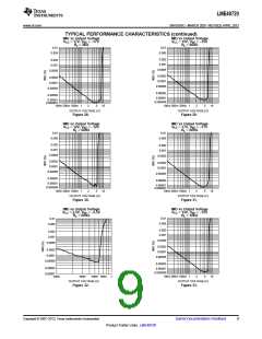
LME49720
SNAS393C –MARCH 2007–REVISED APRIL 2013
www.ti.com
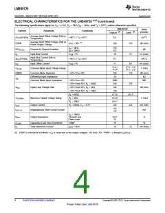
ELECTRICAL CHARACTERISTICS FOR THE LME49720 (1)(2) (continued)
The following specifications apply for VS = ±15V, RL = 2kΩ, fIN = 1kHz, and TA = 25°C, unless otherwise specified.
LME49720
Units
(Limits)
Symbol
Parameter
Conditions
–40°C ≤ TA ≤ 85°C
(3)
(4)
Typical
Limit
Average Input Offset Voltage Drift vs
Temperature
ΔVOS/ΔTemp
0.2
μV/°C
Average Input Offset Voltage Shift vs
Power Supply Voltage
(5)
PSRR
ΔVS = 20V
120
110
dB (min)
fIN = 1kHz
fIN = 20kHz
118
112
ISOCH-CH
IB
Channel-to-Channel Isolation
dB
Input Bias Current
VCM = 0V
10
0.1
11
72
65
nA (max)
nA/°C
Input Bias Current Drift vs
Temperature
ΔIOS/ΔTemp
IOS
–40°C ≤ TA ≤ 85°C
Input Offset Current
VCM = 0V
nA (max)
V (min)
+14.1
–13.9
(V+) – 2.0
(V-) + 2.0
VIN-CM
CMRR
Common-Mode Input Voltage Range
Common-Mode Rejection
–10V<Vcm<10V
120
30
110
125
dB (min)
kΩ
Differential Input Impedance
Common Mode Input Impedance
ZIN
–10V<Vcm<10V
1000
140
MΩ
–10V<Vout<10V, RL = 600Ω
–10V<Vout<10V, RL = 2kΩ
–10V<Vout<10V, RL = 10kΩ
RL = 600Ω
AVOL
Open Loop Voltage Gain
140
dB (min)
V (min)
140
±13.6
±14.0
±14.1
±26
±12.5
±23
VOUTMAX
Maximum Output Voltage Swing
RL = 2kΩ
RL = 10kΩ
IOUT
Output Current
RL = 600Ω, VS = ±17V
mA (min)
mA
+53
–42
IOUT-CC
Instantaneous Short Circuit Current
fIN = 10kHz
Closed-Loop
Open-Loop
ROUT
Output Impedance
0.01
13
Ω
CLOAD
IS
Capacitive Load Drive Overshoot
Total Quiescent Current
100pF
16
10
%
IOUT = 0mA
12
mA (max)
(5) PSRR is measured as follows: VOS is measured at two supply voltages, ±5V and ±15V. PSRR = | 20log(ΔVOS/ΔVS) |.
4
Submit Documentation Feedback
Copyright © 2007–2013, Texas Instruments Incorporated
Product Folder Links: LME49720

 TI [ TEXAS INSTRUMENTS ]