LME49720
www.ti.com
SNAS393C –MARCH 2007–REVISED APRIL 2013
(1)(2)(3)
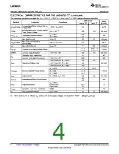
ABSOLUTE MAXIMUM RATINGS
Power Supply Voltage
(VS = V+ - V-)
36V
−65°C to 150°C
(V-) - 0.7V to (V+) + 0.7V
Continuous
Storage Temperature
Input Voltage
(4)
Output Short Circuit
Power Dissipation
Internally Limited
2000V
(5)
ESD Susceptibility
(6)
ESD Susceptibility
Pins 1, 4, 7 and 8
Pins 2, 3, 5 and 6
200V
100V
Junction Temperature
Thermal Resistance
150°C
θJA (SOIC)
θJA (PDIP)
θJA (TO-99)
θJC (TO-99)
145°C/W
102°C/W
150°C/W
35°C/W
Temperature Range
TMIN ≤ TA ≤ TMAX
–40°C ≤ TA ≤ 85°C
±2.5V ≤ VS ≤ ± 17V
Supply Voltage Range
(1) Absolute Maximum Ratings indicate limits beyond which damage to the device may occur.
(2) Operating Ratings indicate conditions for which the device is functional, but do not ensure specific performance limits. For enusred
specifications and test conditions, see Electrical Characteristics. The ensured specifications apply only for the test conditions listed.
Some performance characteristics may degrade when the device is not operated under the listed test conditions.
(3) If Military/Aerospace specified devices are required, please contact the Texas Instruments Sales Office/ Distributors for availability and
specifications.
(4) Amplifier output connected to GND, any number of amplifiers within a package.
(5) Human body model, 100pF discharged through a 1.5kΩ resistor.
(6) Machine Model ESD test is covered by specification EIAJ IC-121-1981. A 200pF cap is charged to the specified voltage and then
discharged directly into the IC with no external series resistor (resistance of discharge path must be under 50Ω).
(1)(2)
ELECTRICAL CHARACTERISTICS FOR THE LME49720
The following specifications apply for VS = ±15V, RL = 2kΩ, fIN = 1kHz, and TA = 25°C, unless otherwise specified.
LME49720
Units
(Limits)
Symbol
Parameter
Conditions
(3)
(4)
Typical
Limit
AV = 1, VOUT = 3Vrms
THD+N
Total Harmonic Distortion + Noise
Intermodulation Distortion
RL = 2kΩ
RL = 600Ω
0.00003
0.00003
% (max)
0.00009
AV = 1, VOUT = 3VRMS
Two-tone, 60Hz & 7kHz 4:1
IMD
0.00005
%
GBWP
SR
Gain Bandwidth Product
Slew Rate
55
45
MHz (min)
±20
±15
V/μs (min)
VOUT = 1VP-P, –3dB
referenced to output magnitude
at f = 1kHz
FPBW
ts
Full Power Bandwidth
10
MHz
AV = –1, 10V step, CL = 100pF
0.1% error range
Settling time
1.2
μs
Equivalent Input Noise Voltage
fBW = 20Hz to 20kHz
0.34
0.65
4.7
μVRMS
(max)
en
f = 1kHz
f = 10Hz
2.7
6.4
nV/√Hz
(max)
Equivalent Input Noise Density
f = 1kHz
f = 10Hz
1.6
3.1
in
Current Noise Density
Offset Voltage
pA/√Hz
VOS
±0.1
±0.7
mV (max)
(1) Absolute Maximum Ratings indicate limits beyond which damage to the device may occur.
(2) Operating Ratings indicate conditions for which the device is functional, but do not ensure specific performance limits. For enusred
specifications and test conditions, see Electrical Characteristics. The ensured specifications apply only for the test conditions listed.
Some performance characteristics may degrade when the device is not operated under the listed test conditions.
(3) Typical specifications are specified at +25ºC and represent the most likely parametric norm.
(4) Tested limits are ensured to AOQL (Average Outgoing Quality Level).
Copyright © 2007–2013, Texas Instruments Incorporated
Submit Documentation Feedback
3
Product Folder Links: LME49720

 TI [ TEXAS INSTRUMENTS ]