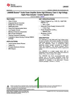
LM48580
www.ti.com
SNAS491A –FEBRUARY 2010–REVISED MAY 2013
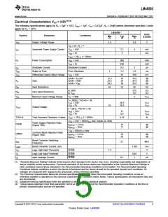
Electrical Characteristics VDD = 3.6V(1)(2)
The following specifications apply for RL = 6μF + 10Ω, CBST = 1μF, CIN = 0.47μF, AV = 24dB unless otherwise specified. Limits
apply for TA = 25°C.
LM48580
Units
Symbol
VDD
Parameter
Conditions
Min
Typ
Max
(Limits)
(3)
(4)
(3)
Supply Voltage Range
2.5
5.5
4
V
VIN = 0V, RL = ∞
IDD
Quiescent Power Supply Current
Power Consumption
VDD = 3.6V
2.7
3
mA
mA
VDD = 3V
VOUT = 25P-P, f = 200Hz
VDD = 3.6V
PD
800
830
0.5
1.4
63
mW
mW
µA
VDD = 3V
ISD
Shutdown Current
Shutdown Enabled
From Shutdown
VDD = 3.6V
2
TWU
VOS
Wake-up Time
1
1.6
360
ms
Differential Output Offset Voltage
mV
GAIN = FLOAT
GAIN = GND
GAIN = VDD
17.5
23.5
29.5
18
24
30
18.5
24.5
30.5
dB
dB
dB
AV
Gain
RIN
RIN
VIN
Input Resistance
46
52
58
kΩ
to GND
to VDD
575
131
kΩ
kΩ
Gain Input Resistance
Maximum Input Voltage Range
AV = 18dB
3
VP-P
f = 200Hz, THD+N = 1%
VDD = 3.6V
VDD = 3V
30.5
30.5
VP-P
VP-P
25
VOUT
Output Voltage
f = 2kHz, THD+N = 5%
VDD = 3.6V
11
8.5
VP-P
VP-P
VDD = 3V
THD+N
PSRR
Total Harmonic Distortion + Noise VOUT = 25VP-P, f = 200Hz
0.16
%
VDD = 3.6V + 200mVp-p sine, Inputs AC GND
Power Supply Rejection Ratio
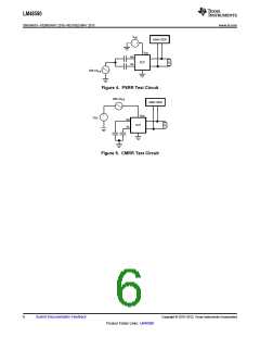
(Figure TBD)
fRIPPLE = 217Hz,
fRIPPLE = 1kHz
75
71
dB
dB
VCM = 200mVP-P sine
Common Mode Rejection Ratio
(Figure TBD)
CMRR
fSW
fRIPPLE = 217Hz
fRIPPLE = 1kHz
56
55
dB
dB
Boost Converter Switching
Frequency
2.1
MHz
ILIMIT
VIH
VIL
Boost Converter Current Limit
Logic High Input Threshold
Logic Low Input Threshold
Input Leakage Current
1100
mA
V
SHDN
SHDN
SHDN
1.2
0.45
1
V
IIN
0.1
μA
(1) “Absolute Maximum Ratings” indicate limits beyond which damage to the device may occur, including inoperability and degradation of
device reliability and/or performance. Functional operation of the device and/or non-degradation at the Absolute Maximum Ratings or
other conditions beyond those indicated in the Recommended Operating Conditions is not implied. The Recommended Operating
Conditions indicate conditions at which the device is functional and the device should not be operated beyond such conditions. All
voltages are measured with respect to the ground pin, unless otherwise specified.
(2) The Electrical Characteristics tables list ensured specifications under the listed Recommended Operating Conditions except as
otherwise modified or specified by the Electrical Characteristics Conditions and/or Notes. Typical specifications are estimations only and
are not ensured.
(3) Datasheet min/max specification limits are specified by design, test, or statistical analysis.
(4) Typical values represent most likely parametric norms at TA = +25ºC, and at the Recommended Operation Conditions at the time of
product characterization and are not specified.
Copyright © 2010–2013, Texas Instruments Incorporated
Submit Documentation Feedback
5
Product Folder Links: LM48580

 TI [ TEXAS INSTRUMENTS ]