LM48580
www.ti.com
SNAS491A –FEBRUARY 2010–REVISED MAY 2013
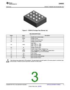
Figure 3. YZR0012 Package View (Bumps Up)
PIN DESCRIPTIONS
Bump
Name
OUT+
SGND
IN+
Description
A1
A2
A3
B1
Amplifier Non-Inverting Output
Amplifier Ground
Amplifier Non-Inverting Input
Amplifier Inverting Output
OUT-
Gain Select:
GAIN = float: AV = 18dB
GAIN = GND: AV = 24dB
GAIN = VDD: AV = 30dB
B2
GAIN
B3
C1
IN-
Amplifier Inverting Input
VAMP
Amplifier Supply Voltage. Connect to VBST
Active Low Shutdown. Drive SHDN low to disable device.
Connect SHDN to VDD for normal operation.
C2
SHDN
C3
D1
D2
D3
VDD
VBST
SW
Power Supply
Boost Converter Output
Boost Converter Switching Node
Boost Converter Ground
PGND
These devices have limited built-in ESD protection. The leads should be shorted together or the device placed in conductive foam
during storage or handling to prevent electrostatic damage to the MOS gates.
Copyright © 2010–2013, Texas Instruments Incorporated
Submit Documentation Feedback
3
Product Folder Links: LM48580

 TI [ TEXAS INSTRUMENTS ]