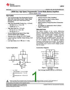
LM359
SNOSBT4C –MAY 1999–REVISED MARCH 2013
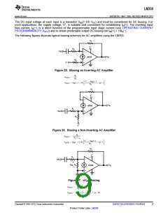
www.ti.com
These devices have limited built-in ESD protection. The leads should be shorted together or the device placed in conductive foam
during storage or handling to prevent electrostatic damage to the MOS gates.
Absolute Maximum Ratings(1)(2)
Supply Voltage
22 VDC or ±11 VDC
1W
D Package
Power Dissipation(3)
NFF Package
D Package
750 mW
+150°C
Maximum TJ
NFF Package
+125°C
147°C/W still air
D Package θjA
110°C/W with 400
linear feet/min air flow
Thermal Resistance
100°C/W still air
NFF Package θjA
75°C/W with 400
linear feet/min air flow
Input Currents, IIN(+) or IIN(−)
Set Currents, ISET(IN) or ISET(OUT)
Operating Temperature Range
Storage Temperature Range
Lead Temperature
10 mADC
2 mADC
0°C to +70°C
−65°C to +150°C
260°C
(Soldering, 10 sec.)
Soldering (10 sec.)
Vapor Phase (60 sec.)
Infrared (15 sec.)
PDIP Package
SOIC Package
260°C
Soldering Information
215°C
220°C
(1) “Absolute Maximum Ratings” indicate limits beyond which damage to the device may occur. Operating Ratings indicate conditions for
which the device is functional, but do not ensure specific performance limits.
(2) If Military/Aerospace specified devices are required, please contact the Texas Instruments Sales Office/ Distributors for availability and
specifications.
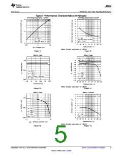
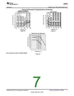
(3) See Figure 22.
Electrical Characteristics
ISET(IN) = ISET(OUT) = 0.5 mA, Vsupply = 12V, TA = 25°C unless otherwise noted
Parameter
Open Loop Voltage
Gain
Conditions
Vsupply = 12V, RL = 1k, f = 100 Hz
Min
Typ
72
Max
Units
dB
62
TA = 125°C
68
dB
Bandwidth Unity Gain
RIN = 1 kΩ, Ccomp = 10 pF
15
30
MHz
Gain Bandwidth Product,
Gain of 10 to 100
RIN = 50Ω to 200Ω
200
400
MHz
V/μs
dB
Unity Gain
RIN = 1 kΩ, Ccomp = 10 pF
RIN < 200Ω
30
60
Slew Rate
Gain of 10 to 100
Amplifier to Amplifier
Coupling
f = 100 Hz to 100 kHz, RL = 1k
−80
at 2 mA IIN(+), ISET = 5 μA, TA = 25°C
at 0.2 mA IIN(+), ISET = 5 μA Over Temp.
at 20 μA IIN(+), ISET = 5 μA Over Temp.
0.9
0.9
0.9
1.0
1.0
1.0
3
1.1
1.1
1.1
5
μA/μA
μA/μA
μA/μA
%
Mirror Gain(1)
ΔMirror Gain(1)
at 20 μA to 0.2 mA IIN(+) Over Temp, ISET = 5 μA
Inverting Input, TA = 25°C
Over Temp.
8
15
30
μA
Input Bias Current
μA
Input Resistance (βre)
Inverting Input
2.5
3.5
kΩ
Output Resistance
IOUT = 15 mA rms, f = 1 MHz
Ω
(1) Mirror gain is the current gain of the current mirror which is used as the non-inverting input.
AI for two different mirror currents at any given temperature.
ΔMirror Gain is the % change in
2
Submit Documentation Feedback
Copyright © 1999–2013, Texas Instruments Incorporated
Product Folder Links: LM359

 TI [ TEXAS INSTRUMENTS ]