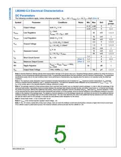
LM2990-5.0 Electrical Characteristics
DC Parameters
The following conditions apply, unless otherwise specified. VIN = −5V + VO Nom, IO = 1A, CO = 47µF (Note 6)
Sub-
groups
Symbol
VO
VRLine
VRLoad
Parameter
Output Voltage
Conditions
Notes
Min Max
Unit
-5.10 -4.90
-5.25 -4.75
V
V
1
5mA ≤ IO ≤ 1A
2, 3
IO = 5mA,
Line Regulation
Load Regulation
40
mV
1, 2, 3
VO Nom -1V > VIN > -26V
70
100
0.3
mV
mV
V
1
50mA ≤ IO ≤ 1A
2, 3
1, 2, 3
IO = 0.1A, ΔVO ≤ 100mV
IO = 1A, ΔVO ≤ 100mV
VDO
Dropout Voltage
1.0
V
1, 2, 3
5.0
mA
mA
mA
A
1
2, 3
1, 2, 3
1
IO ≤ 1A
IQ
10
50
Quiescent Current
IO = 1A, VIN = VO Nom
1.5
IOS
Short Circuit Current
Maximum Output Current
Ripple Rejection
RL = 1Ω
(Note 7)
(Note 7)
1.3
A
2, 3
1
IMax
RR
VOn
1.5
A
VRipple = 1VRMS, FRipple = 1KHz,
IO = 5mA
50
dB
µV
1
Output Noise Voltage
10Hz-100Khz, IO = 5mA
750
1, 2, 3
Note 2: Absolute Maximum Ratings indicate limits beyond which damage to the device may occur. Operating Ratings indicate conditions for which the device is
functional, but do not guarantee specific performance limits. For guaranteed specifications and test conditions, see the Electrical Characteristics. The guaranteed
specifications apply only for the test conditions listed. Some performance characteristics may degrade when the device is not operated under the listed test
conditions.
Note 3: The maximum power dissipation must be derated at elevated temperatures and is dictated by TJmax (maximum junction temperature), θJA (package
junction to ambient thermal resistance), and TA (ambient temperature). The maximum allowable power dissipation at any temperature is PDmax = (TJmax - TA)/
θ
JA or the number given in the Absolute Maximum Ratings, whichever is lower.
Note 4: The package material for these devices allows much improved heat transfer over our standard ceramic packages. In order to take full advantage of this
improved heat transfer, heat sinking must be provided between the package base (directly beneath the die), and either metal traces on, or thermal vias through,
the printed circuit board. Without this additional heat sinking, device power dissipation must be calculated using θJA, rather than θJC, thermal resistance. It must
not be assumed that the device leads will provide substantial heat transfer out of the package, since the thermal resistance of the leadframe material is very poor,
relative to the material of the package base. The stated θJC thermal resistance is for the package material only, and does not account for the additional thermal
resistance between the package base and the printed circuit board. The user must determine the value of the additional thermal resistance and must combine
this with the stated value for the package, to calculate the total allowed power dissipation for the device.
Note 5: Human body model, 1.5 kΩ in series with 100 pF.
Note 6: VO Nom is the nominal (typical) regulator output voltage, −5V.
Note 7: The −5V version, tested with a lower input voltage, does not reach the foldback current limit and therefore conducts a higher short circuit current level.
If the LM2990 output is pulled above ground, the maximum allowed current sunk back into the LM2990 is 1.5A.
www.national.com
4

 TI [ TEXAS INSTRUMENTS ]