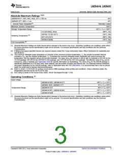
LM2940-N, LM2940C
www.ti.com
SNVS769I –MARCH 2000–REVISED APRIL 2013
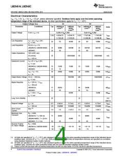
Electrical Characteristics (continued)
VIN = VO + 5V, IO = 1A, CO = 22 μF, unless otherwise specified. Boldface limits apply over the entire operating
temperature range of the indicated device. All other specifications apply for TA = TJ = 25°C.
Output Voltage (VO)
Parameter Conditions
12V
15V
Typ
LM2940-N
LM2940-
N/833
Limit
Typ
LM2940-N
LM2940-
N/833
Limit
Units
(1)
(1)
Limit
Limit
(2)
(2)
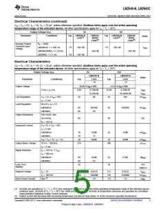
Ripple Rejection
fO = 120 Hz, 1 Vrms
IO = 100 mA
LM2940-N
,
66
66
54/48
dBMIN
dBMIN
LM2940C
54
64
60
52
fO = 1 kHz, 1 Vrms
IO = 5 mA
,
52/46
48/42
Long Term Stability
Dropout Voltage
mV/
1000 Hr
48
IO = 1A
0.5
110
1.9
0.8/1.0
150/200
1.6
0.7/1.0
150/200
1.6/1.3
0.5
110
1.9
0.8/1.0
150/200
1.6
0.7/1.0
150/200
1.6/1.3
VMAX
mVMAX
AMIN
IO = 100 mA
(3)
Short Circuit Current See
Maximum Line
Transient
RO = 100Ω
LM2940-N, T ≤ 100 ms
LM2940-N/883, T ≤ 20 ms
LM2940C, T ≤ 1 ms
RO = 100Ω
75
55
60/60
40/40
40/40
VMIN
45
55
45
Reverse Polarity
DC Input Voltage
LM2940-N, LM2940-N/883
LM2940C
−30
−30
−15/−15
−15
−15/−15
−15/−15
VMIN
−30
−15
Reverse Polarity
Transient Input
Voltage
RO = 100Ω
LM2940-N, T ≤ 100 ms
LM2940-N/883, T ≤ 20 ms
LM2940C, T ≤ 1 ms
−75
−50/−50
−45/−45
−45/−45
VMIN
−55
−45/−45
−55
−45/−45
(3) Output current will decrease with increasing temperature but will not drop below 1A at the maximum specified temperature.
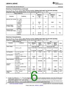
Thermal Performance
3-Lead TO-220
4
4
Thermal Resistance
Junction-to-Case, θ(JC)
°C/W
3-Lead DDPAK/TO-263
(1)
3-Lead TO-220
60
80
174
35
(1)
3-Lead DDPAK/TO-263
SOT-223(1)
Thermal Resistance
Junction-to-Ambient, θ(JA)
°C/W
(1)
8-Lead WSON
(1) The maximum allowable power dissipation is a function of the maximum junction temperature, TJ, the junction-to-ambient thermal
resistance, θJA, and the ambient temperature, TA. Exceeding the maximum allowable power dissipation will cause excessive die
temperature, and the regulator will go into thermal shutdown. The value of θJA (for devices in still air with no heatsink) is 60°C/W for the
TO-220 package, 80°C/W for the DDPAK/TO-263 package, and 174°C/W for the SOT-223 package. The effective value of θJA can be
reduced by using a heatsink (see Application Hints for specific information on heatsinking). The value of θJA for the WSON package is
specifically dependent on PCB trace area, trace material, and the number of layers and thermal vias. For improved thermal resistance
and power dissipation for the WSON package, refer to Application Note AN-1187 (SNOA401). It is recommended that 6 vias be placed
under the center pad to improve thermal performance.
Copyright © 2000–2013, Texas Instruments Incorporated
Submit Documentation Feedback
7
Product Folder Links: LM2940-N LM2940C

 TI [ TEXAS INSTRUMENTS ]