LM2940-N, LM2940C
www.ti.com
SNVS769I –MARCH 2000–REVISED APRIL 2013
(1)(2)
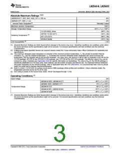
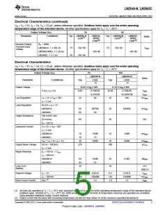
Absolute Maximum Ratings
LM2940-N KTT, NFE, NAC, NDE, DCY ≤ 100 ms
60V
45V
LM2940C KTT, NDE ≤ 1 ms
Internal Power Dissipation(3)
Internally Limited
150°C
Maximum Junction Temperature
Storage Temperature Range
−65°C ≤ TJ ≤ +150°C
260°C, 10s
235°C, 30s
260°C, 30s
235°C, 30s
2 kV
TO-220 (NDE), Wave
DDPAK/ TO-263 (KTT)
SOT-223 (DCY)
(4)
Soldering Temperature
WSON-8 (NGN)
(5)
ESD Susceptibility
(1) Absolute Maximum Ratings are limits beyond which damage to the device may occur. Operating Conditions are conditions under which
the device functions but the specifications might not be ensured. For ensured specifications and test conditions see the Electrical
Characteristics.
(2) If Military/Aerospace specified devices are required, please contact the Texas Instruments Sales Office/ Distributors for availability and
specifications.
(3) The maximum allowable power dissipation is a function of the maximum junction temperature, TJ, the junction-to-ambient thermal
resistance, θJA, and the ambient temperature, TA. Exceeding the maximum allowable power dissipation will cause excessive die
temperature, and the regulator will go into thermal shutdown. The value of θJA (for devices in still air with no heatsink) is 60°C/W for the
TO-220 package, 80°C/W for the DDPAK/TO-263 package, and 174°C/W for the SOT-223 package. The effective value of θJA can be
reduced by using a heatsink (see Application Hints for specific information on heatsinking). The value of θJA for the WSON package is
specifically dependent on PCB trace area, trace material, and the number of layers and thermal vias. For improved thermal resistance
and power dissipation for the WSON package, refer to Application Note AN-1187 (SNOA401). It is recommended that 6 vias be placed
under the center pad to improve thermal performance.
(4) Refer to JEDEC J-STD-020C for surface mount device (SMD) package reflow profiles and conditions. Unless otherwise stated, the
temperature and time are for Sn-Pb (STD) only.
(5) ESD rating is based on the human body model, 100 pF discharged through 1.5 kΩ.
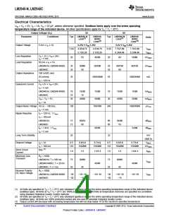
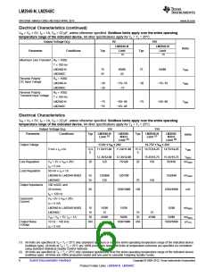
(1)
Operating Conditions
Input Voltage
26V
−40°C ≤ TJ ≤ 125°C
0°C ≤ TJ ≤ 125°C
LM2940-N NDE, LM2940-N KTT
LM2940C NDE, LM2940C KTT
LM2940-N DCY
Temperature Range
−40°C ≤ TA ≤ 85°C
−55°C ≤ TJ ≤ 125°C
−40°C ≤ TJ ≤ 125°C
LM2940-N NFE, LM2940-N NAC
LM2940-N NGN
(1) Absolute Maximum Ratings are limits beyond which damage to the device may occur. Operating Conditions are conditions under which
the device functions but the specifications might not be ensured. For ensured specifications and test conditions see the Electrical
Characteristics.
Copyright © 2000–2013, Texas Instruments Incorporated
Submit Documentation Feedback
3
Product Folder Links: LM2940-N LM2940C

 TI [ TEXAS INSTRUMENTS ]