LM27761
www.ti.com.cn
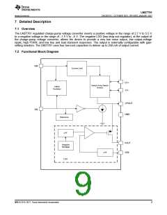
ZHCSEO7C –OCTOBER 2015–REVISED JANUARY 2017
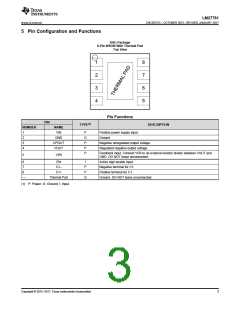
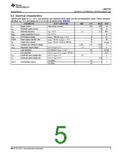
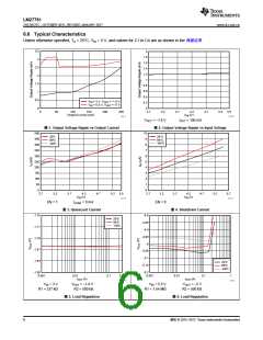
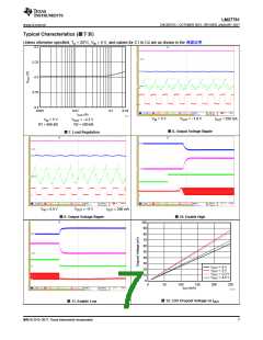
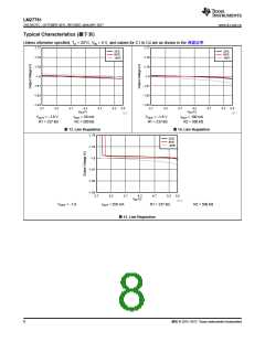
5 Pin Configuration and Functions
DSG Package
8-Pin WSON With Thermal Pad
Top View
1
8
7
6
5
2
3
4
Pin Functions
PIN
TYPE(1)
DESCRIPTION
NUMBER
NAME
VIN
1
2
3
4
P
G
P
P
P
Positive power supply input.
Ground
GND
CPOUT
VOUT
Negative unregulated output voltage.
Regulated negative output voltage.
Feedback input. Connect VFB to an external resistor divider between VOUT and
GND. DO NOT leave unconnected.
5
VFB
6
EN
C1–
I
Active high enable input.
7
P
P
G
Negative terminal for C1.
8
C1+
Positive terminal for C1.
—
Thermal Pad
Ground. DO NOT leave unconnected.
(1) P: Power; G: Ground; I: Input.
Copyright © 2015–2017, Texas Instruments Incorporated
3

 TI [ TEXAS INSTRUMENTS ]