LM2672
www.ti.com
SNVS136K –SEPTEMBER 1998–REVISED APRIL 2013
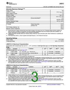
Absolute Maximum Ratings(1)(2)
Supply Voltage
45V
−0.1V ≤ VSH ≤ 6V
−1V
ON/OFF Pin Voltage
Switch Voltage to Ground
Boost Pin Voltage
VSW + 8V
Feedback Pin Voltage
ESD Susceptibility
−0.3V ≤ VFB ≤ 14V
2 kV
Human Body Model(3)
Power Dissipation
Internally Limited
−65°C to +150°C
Storage Temperature Range
Lead Temperature
D Package
Vapor Phase (60s)
Infrared (15s)
+215°C
+220°C
+260°C
+150°C
PDIP Package (Soldering, 10s)
Maximum Junction Temperature
(1) Absolute Maximum Ratings indicate limits beyond which damage to the device may occur. Operating Ratings indicate conditions for
which the device is intended to be functional, but device parameter specifications may not be ensured under these conditions. For
specific specifications and test conditions, see the Electrical Characteristics.
(2) If Military/Aerospace specified devices are required, please contact the Texas Instruments Sales Office/ Distributors for availability and
specifications.
(3) The human body model is a 100 pF capacitor discharged through a 1.5 kΩ resistor into each pin.
Operating Ratings
Supply Voltage
6.5V to 40V
Temperature Range
−40°C ≤ TJ ≤ +125°C
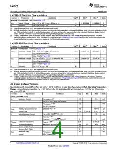
LM2672-3.3 Electrical Characteristics
Specifications with standard type face are for TJ = 25°C, and those in bold type face apply over full Operating Temperature
Range.
Symbol
Parameter
Conditions
Typ(1)
Min(2)
Max(2)
Units
SYSTEM PARAMETERS Test Circuit Figure 22(3)
VOUT
VOUT
η
Output Voltage
Output Voltage
Efficiency
VIN = 8V to 40V, ILOAD = 20 mA to 1A
VIN = 6.5V to 40V, ILOAD = 20 mA to 500 mA
VIN = 12V, ILOAD = 1A
3.3
3.3
86
3.251/3.201
3.251/3.201
3.350/3.399
3.350/3.399
V
V
%
(1) Typical numbers are at 25°C and represent the most likely norm.
(2) All limits specified at room temperature (standard type face) and at temperature extremes (bold type face). All room temperature limits
are 100% production tested. All limits at temperature extremes are specified via correlation using standard Statistical Quality Control
(SQC) methods. All limits are used to calculate Average Outgoing Quality Level (AOQL).
(3) External components such as the catch diode, inductor, input and output capacitors, and voltage programming resistors can affect
switching regulator performance. When the LM2672 is used as shown in Figure 22 and Figure 23 test circuits, system performance will
be as specified by the system parameters section of the Electrical Characteristics.
LM2672-5.0 Electrical Characteristics
Symbol
Parameter
Conditions
Typ(1)
Min(2)
Max(2)
Units
SYSTEM PARAMETERS Test Circuit Figure 22(3)
VOUT
VOUT
η
Output Voltage
Output Voltage
Efficiency
VIN = 8V to 40V, ILOAD = 20 mA to 1A
VIN = 6.5V to 40V, ILOAD = 20 mA to 500 mA
VIN = 12V, ILOAD = 1A
5.0
5.0
90
4.925/4.850
4.925/4.850
5.075/5.150
5.075/5.150
V
V
%
(1) Typical numbers are at 25°C and represent the most likely norm.
(2) All limits specified at room temperature (standard type face) and at temperature extremes (bold type face). All room temperature limits
are 100% production tested. All limits at temperature extremes are specified via correlation using standard Statistical Quality Control
(SQC) methods. All limits are used to calculate Average Outgoing Quality Level (AOQL).
(3) External components such as the catch diode, inductor, input and output capacitors, and voltage programming resistors can affect
switching regulator performance. When the LM2672 is used as shown in Figure 22 and Figure 23 test circuits, system performance will
be as specified by the system parameters section of the Electrical Characteristics.
Copyright © 1998–2013, Texas Instruments Incorporated
Submit Documentation Feedback
3
Product Folder Links: LM2672

 TI [ TEXAS INSTRUMENTS ]