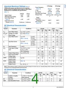
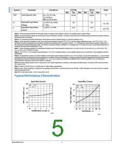
LF412A
Typ
LF412
Typ
Symbol
Parameter
Conditions
Units
Min
Max
Min
Max
THD
Total Harmonic Dist
AV=+10, RL=10k,
VO=20 Vp-p,
%
≤0.02
≤0.02
BW=20 Hz-20 kHz
en
in
Equivalent Input Noise
Voltage
TA=25°C, RS=100Ω,
f=1 kHz
25
25
Equivalent Input Noise
Current
TA=25°C, f=1 kHz
0.01
0.01
Note 3: Unless otherwise specified the absolute maximum negative input voltage is equal to the negative power supply voltage.
Note 4: Any of the amplifier outputs can be shorted to ground indefintely, however, more than one should not be simultaneously shorted as the maximum junction
temperature will be exceeded.
Note 5: For operating at elevated temperature, these devices must be derated based on a thermal resistance of θjA.
Note 6: These devices are available in both the commercial temperature range 0°C≤TA≤70°C and the military temperature range −55°C≤TA≤125°C. The
temperature range is designated by the position just before the package type in the device number. A “C” indicates the commercial temperature range and an
“M” indicates the military temperature range. The military temperature range is available in “H” package only. In all cases the maximum operating temperature is
limited by internal junction temperature Tj max.
Note 7: Unless otherwise specified, the specifications apply over the full temperature range and for VS=±20V for the LF412A and for VS=±15V for the LF412.
VOS, IB, and IOS are measured at VCM=0.
Note 8: The LF412A is 100% tested to this specification. The LF412 is sample tested on a per amplifier basis to insure at least 85% of the amplifiers meet this
specification.
Note 9: The input bias currents are junction leakage currents which approximately double for every 10°C increase in the junction temperature, Tj. Due to limited
production test time, the input bias currents measured are correlated to junction temperature. In normal operation the junction temperature rises above the ambient
temperature as a result of internal power dissipation, PD. Tj=TA+θjA PD where θjA is the thermal resistance from junction to ambient. Use of a heat sink is
recommended if input bias current is to be kept to a minimum.
Note 10: Supply voltage rejection ratio is measured for both supply magnitudes increasing or decreasing simultaneously in accordance with common practice.
VS = ±6V to ±15V.
Note 11: Refer to RETS412X for LF412MH and LF412MJ military specifications.
Note 12: Max. Power Dissipation is defined by the package characteristics. Operating the part near the Max. Power Dissipation may cause the part to operate
outside guaranteed limits.
Note 13: Human body model, 1.5 kΩ in series with 100 pF.
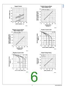
Typical Performance Characteristics
Input Bias Current
Input Bias Current
565610
565611
www.national.com
4

 TI [ TEXAS INSTRUMENTS ]