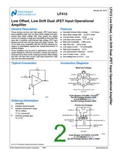
H Package
N Package
Absolute Maximum Ratings (Note 2)
If Military/Aerospace specified devices are required,
please contact the National Semiconductor Sales Office/
Distributors for availability and specifications.
Power Dissipation
ꢀ(Note 12)
Tj max
(Note 5)
150°C
670 mW
115°C
152°C/W
(Note 6)
115°C/W
(Note 6)
θ
jA (Typical)
(Note 11)
Operating Temp. Range
Storage Temp.
LF412A
±22V
±38V
LF412
±18V
±30V
−65°C≤TA≤150° −65°C≤TA≤150°
Supply Voltage
C
C
Differential Input Voltage
Input voltage Range
ꢀ(Note 3)
Output Short Circuit
Duration (Note 4)
Range
Lead Temp.
±19V
±15V
(Soldering, 10 sec.)
ESD Tolerance
ꢀ(Note 13)
260°C
1700V
260°C
1700V
Continuous Continuous
DC Electrical Characteristics
(Note 7)
Symbol
Parameter
Conditions
LF412A
LF412
Typ
Units
Min
Typ
Max Min
Max
VOS
Input Offset Voltage
0.5
1.0
10
1.0
3.0
mV
RS=10 kΩ, TA=25°C
Average TC of Input
Offset Voltage
ΔVOS/ΔT
RS=10 kΩ (Note 8)
7
7
20
μV/°C
IOS
Input Offset Current
VS=±15V
Tj=25°C
Tj=70°C
Tj=125°C
Tj=25°C
Tj=70°C
Tj=125°C
25
100
2
25
100
2
pA
nA
nA
pA
nA
nA
(Note 7, Note 9)
25
200
4
25
200
4
IB
Input Bias Current
VS=±15V
50
50
(Note 7, Note 9)
50
50
RIN
Input Resistance
Large Signal Voltage
Gain
Tj=25°C
1012
200
1012
200
Ω
AVOL
VS=±15V, VO=±10V,
RL=2k, TA=25°C
Over Temperature
VS=±15V, RL=10k
50
25
V/mV
25
200
±13.5
+19.5
−16.5
100
15
200
±13.5
+14.5
−11.5
100
V/mV
V
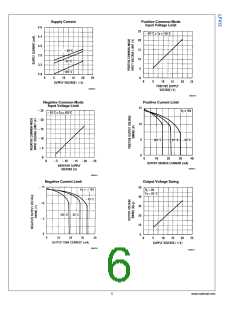
VO
Output Voltage Swing
Input Common-Mode
Voltage Range
±12
±16
±12
±11
VCM
V
V
CMRR
Common-Mode
80
80
70
70
dB
RS≤10k
Rejection Ratio
Supply Voltage
Rejection Ratio
Supply Current
PSRR
IS
(Note 10)
100
3.6
100
3.6
dB
5.6
6.5
mA
VO = 0V, RL = ∞
Note 2: “Absolute Maximum Ratings” indicate limits beyond which damage to the device may occur. Operating Ratings indicate conditions for which the device
is functional, but do not guarantee specific performance limits.
AC Electrical Characteristics
(Note 7)
LF412A
Typ
LF412
Typ
Symbol
Parameter
Conditions
Units
Min
Max
Min
Max
Amplifier to Amplifier
Coupling
TA=25°C, f=1 Hz-20 kHz
(Input Referred)
−120
−120
dB
SR
GBW
Slew Rate
VS=±15V, TA=25°C
VS=±15V, TA=25°C
10
3
15
4
8
15
4
V/μs
MHz
Gain-Bandwidth Product
2.7
3
www.national.com

 TI [ TEXAS INSTRUMENTS ]