LF147, LF347-N
SNOSBH1D –MAY 1999–REVISED MARCH 2013
www.ti.com
This integrated circuit can be damaged by ESD. Texas Instruments recommends that all integrated circuits be handled with
appropriate precautions. Failure to observe proper handling and installation procedures can cause damage.
ESD damage can range from subtle performance degradation to complete device failure. Precision integrated circuits may be more
susceptible to damage because very small parametric changes could cause the device not to meet its published specifications.
(1)(2)
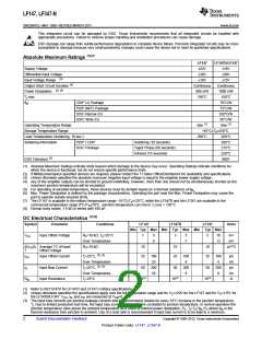
Absolute Maximum Ratings
LF147
±22V
LF347B/LF347
±18V
Supply Voltage
Differential Input Voltage
±38V
±30V
(3)
Input Voltage Range
±19V
±15V
(4)
Output Short Circuit Duration
Continuous
900 mW
150°C
Continuous
1000 mW
150°C
(5) (6)
Power Dissipation
Tj max
θjA
CDIP (J) Package
PDIP (NFF) Package
SOIC Narrow (D)
SOIC Wide (D)
70°C/W
75°C/W
100°C/W
85°C/W
(7)
(7)
Operating Temperature Range
Storage Temperature Range
See
See
−65°C≤TA≤150°C
Lead Temperature (Soldering, 10 sec.)
260°C
260°C
260°C
215°C
220°C
900V
Soldering Information
PDIP / CDIP
SOIC Package
Soldering (10 seconds)
Vapor Phase (60 seconds)
Infrared (15 seconds)
(8)
ESD Tolerance
(1) Absolute Maximum Ratings indicate limits beyond which damage to the device may occur. Operating Ratings indicate conditions for
which the device is functional, but do not ensure specific performance limits.
(2) If Military/Aerospace specified devices are required, please contact the TI Sales Office/Distributors for availability and specifications.
(3) Unless otherwise specified the absolute maximum negative input voltage is equal to the negative power supply voltage.
(4) Any of the amplifier outputs can be shorted to ground indefinitely, however, more than one should not be simultaneously shorted as the
maximum junction temperature will be exceeded.
(5) For operating at elevated temperature, these devices must be derated based on a thermal resistance of θjA.
(6) Max. Power Dissipation is defined by the package characteristics. Operating the part near the Max. Power Dissipation may cause the
part to operate outside ensured limits.
(7) The LF147 is available in the military temperature range −55°C≤TA≤125°C, while the LF347B and the LF347 are available in the
commercial temperature range 0°C≤TA≤70°C. Junction temperature can rise to Tj max = 150°C.
(8) Human body model, 1.5 kΩ in series with 100 pF.
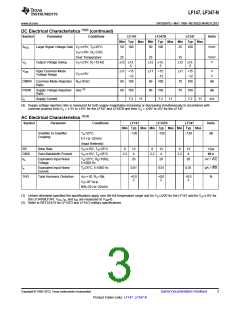
(1)(2)
DC Electrical Characteristics
Symbol
Parameter
Conditions
LF147
LF347B
LF347
Units
Min Typ Max Min Typ Max Min Typ Max
VOS
Input Offset Voltage
RS=10 kΩ, TA=25°C
Over Temperature
RS=10 kΩ
1
5
8
3
5
7
5
10
13
mV
mV
ΔVOS/Δ Average TC of Input
T
10
25
10
25
10
25
μV/°C
Offset Voltage
(2) (3)
IOS
Input Offset Current
Tj=25°C,
100
25
100
4
100
4
pA
nA
pA
nA
Ω
Over Temperature
(2) (3)
IB
Input Bias Current
Input Resistance
Tj=25°C,
50
200
50
50
200
8
50
200
8
Over Temperature
Tj=25°C
RIN
1012
1012
1012
(1) Refer to RETS147X for LF147D and LF147J military specifications.
(2) Unless otherwise specified the specifications apply over the full temperature range and for VS=±20V for the LF147 and for VS=±15V for
the LF347B/LF347. VOS, IB, and IOS are measured at VCM=0.
(3) The input bias currents are junction leakage currents which approximately double for every 10°C increase in the junction temperature,
Tj. Due to limited production test time, the input bias currents measured are correlated to junction temperature. In normal operation the
junction temperature rises above the ambient temperature as a result of internal power dissipation, PD. Tj=TA+θjA PD where θjA is the
thermal resistance from junction to ambient. Use of a heat sink is recommended if input bias current is to be kept to a minimum.
2
Submit Documentation Feedback
Copyright © 1999–2013, Texas Instruments Incorporated
Product Folder Links: LF147 LF347-N

 TI [ TEXAS INSTRUMENTS ]