Absolute Maximum Ratings (Note 1)
If Military/Aerospace specified devices are required,
please contact the National Semiconductor Sales Office/
Distributors for availability and specifications.
Package Derating:
28L SSOP
10.3mW/˚C above +25˚C
>
ESD Rating (HBM)
2kV
Supply Voltage (VCC
)
−0.3V to +4V
−0.3V to (VCC +0.3V)
−0.3V to (VCC +0.3V)
Recommended Operating
Conditions
CMOS/TTL Input Voltage
CMOS/TTL Output Voltage
Bus LVDS Receiver Input
Voltage
Min
Nom Max Units
−0.3V to +3.9V
+150˚C
Supply Voltage (VCC
)
3.0
3.3
3.6
+85
2.4
V
˚C
V
Junction Temperature
Storage Temperature
Lead Temperature
Operating Free Air
Temperature (TA)
−65˚C to +150˚C
−40
0
+25
Receiver Input Range
(Soldering, 4 seconds)
+260˚C
Maximum Package Power Dissipation Capacity
Supply Noise Voltage
100 mVP-P
(VCC
)
@
25˚C Package:
28L SSOP
1.27 W
Electrical Characteristics
Over recommended operating supply and temperature ranges unless otherwise specified.
Symbol
Parameter
Conditions
Min
Typ
Max
Units
DESERIALIZER LVCMOS/LVTTL DC SPECIFICATIONS (apply to pins PWRDN, RCLK_R/ F, REN, REFCLK = inputs; apply to
pins ROUT, RCLK, LOCK = outputs)
VIH
VIL
High Level Input Voltage
Low Level Input Voltage
Input Clamp Voltage
2.0
VCC
0.8
V
V
GND
VCL
IIN
ICL = −18 mA
−0.62
−1.5
+15
VCC
0.5
V
±
Input Current
VIN = 0V or 3.6V
IOH = −9 mA
−10
2.1
2
µA
V
VOH
VOL
IOS
IOZ
High Level Output Voltage
Low Level Output Voltage
Output Short Circuit Current
TRI-STATE Output Current
2.93
0.33
−38
IOL = 9 mA
GND
−15
−10
V
VOUT = 0V
−85
+10
mA
µA
±
PWRDN or REN = 0.8V, VOUT = 0V or VCC
0.4
DESERIALIZER Bus LVDS DC SPECIFICATIONS (apply to pins RI+ and RI−)
VTH
VTL
IIN
Differential Threshold High
Voltage
VCM = +1.1V
+6
+50
mV
mV
Differential Threshold Low
Voltage
−50
−12
±
Input Current
VIN = +2.4V, VCC = 3.6V or 0V
VIN = 0V, VCC = 3.6V or 0V
−10
−10
1
+15
+10
µA
µA
±
0.05
DESERIALIZER SUPPLY CURRENT (apply to pins DVCC and AVCC)
ICCR
Deserializer Supply Current
Worst Case
CL = 15 pF
Figure 1
f = 40 MHz
f = 16 MHz
58
30
75
45
mA
mA
ICCXR
Deserializer Supply Current
Powerdown
PWRDN = 0.8V, REN = 0.8V
0.36
1.0
mA
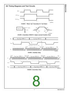
Deserializer Timing Requirements for REFCLK
Over recommended operating supply and temperature ranges unless otherwise specified.
Symbol
tRFCP
tRFDC
fRef
Parameter
REFCLK Period
Conditions
Min
Typ
T
Max
Units
25
62.5
ns
%
REFCLK Duty Cycle
REFCLK Frequency
REFCLK Transition Time
50
tRCP
3
0.95/tRCP
1.05/tRCP
6
tRFTT
ns
5
www.national.com

 TI [ TEXAS INSTRUMENTS ]